



Groundbreaking Semiconductor Research Enables Direct Observation of Chemical Changes at Wiring Interfaces
Groundbreaking Research in Semiconductor Technology
Introduction
In a remarkable advancement in semiconductor research, the Toray Research Center (TRC) and Professor Masaki Tanabe from the Shibaura Institute of Technology have made a significant discovery. They utilized Atomic Force Microscopy Infrared (AFM-IR) spectroscopy to visualize minute chemical structure changes occurring near the interfaces of copper (Cu) wiring and low-k dielectric materials within semiconductor devices. This achievement opens new avenues for understanding device performance degradation related to these chemical interactions.
The Challenge with Traditional Methods
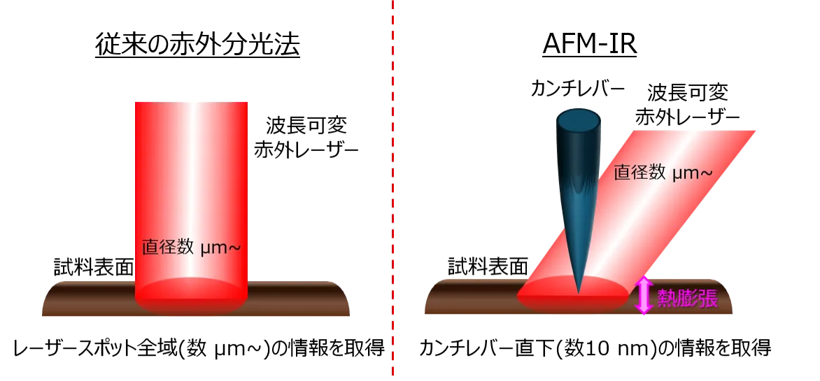
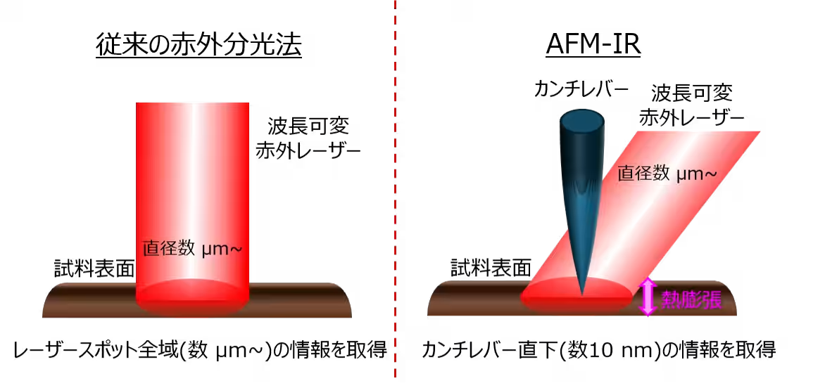
Previously, traditional infrared spectroscopy methods struggled to provide detailed insights into localized chemical changes within real semiconductor wiring structures. The broad measurement areas led to signals being averaged out, making it nearly impossible to assess the subtle chemical variations that occur within nanometer-scale zones close to Cu wiring. Moreover, while electron microscopy could analyze elements, it had limitations concerning functional group-level chemical structure analysis.
Recognizing a Novel Approach
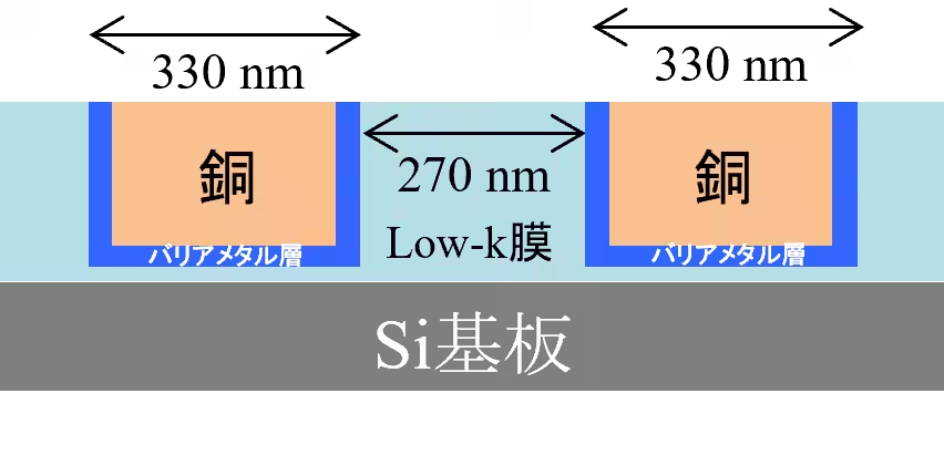
To overcome these limitations, TRC and Professor Tanabe focused on AFM-IR, a technique capable of conducting chemical analysis at the nanometer scale. Their research concentrated on a Cu/low-k dielectric substrate model, aiming to reveal the significance of the chemical changes associated with semiconductor wiring structures.
Significant Findings
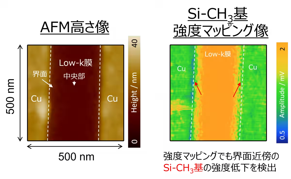
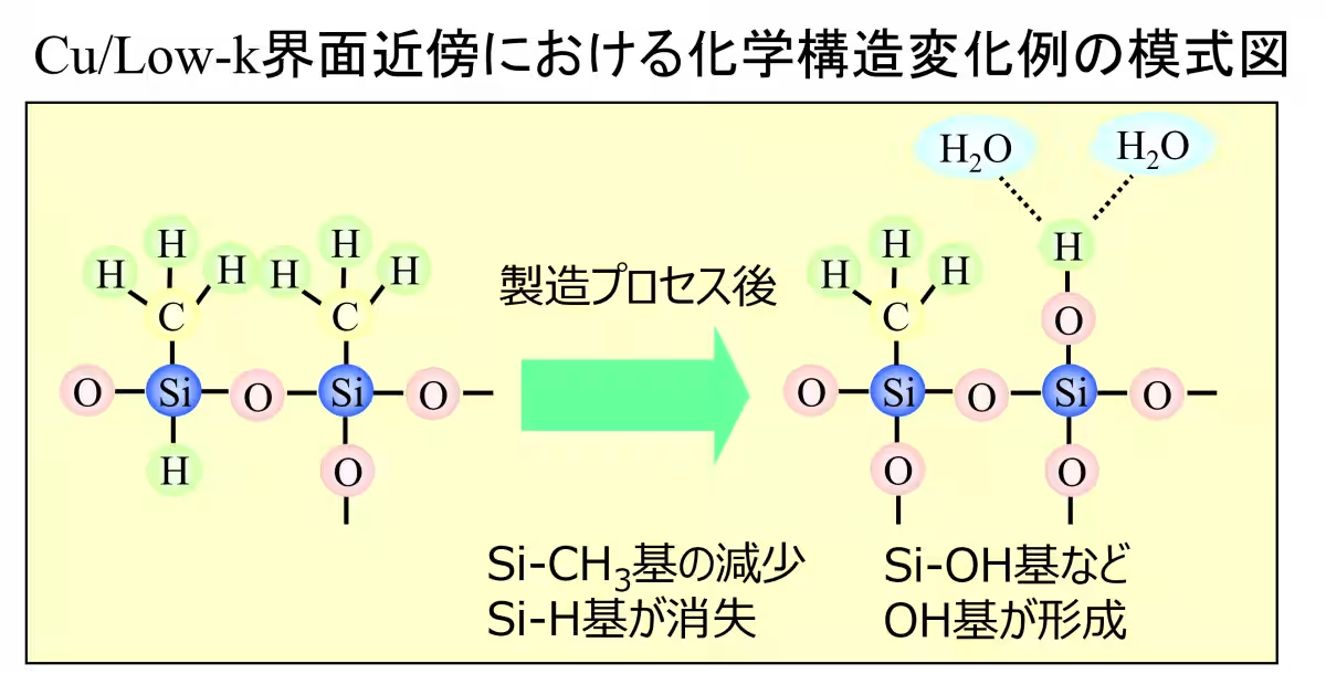
Through their measurements, they discovered that near the Cu wiring, crucial components like the methyl group (Si-CH₃) and Si-H bonds, essential for maintaining low-k dielectric material performance, decreased in density. In contrast, components associated with hydroxyl (OH) groups increased. These changes can potentially lead to a decline in dielectric properties, serving as critical information for better understanding the factors contributing to semiconductor device performance degradation.
Visualizing Chemical Changes
The ability to directly visualize these localized chemical changes represents a substantial leap forward in semiconductor analysis and quality control. The findings confirmed that the chemical alterations were primarily concentrated within very narrow regions, around tens of nanometers from the interface—insight that traditional methods could not achieve.
Implications for Semiconductor Manufacturing
The implications of this research are profound for the semiconductor industry. The newly established AFM-IR interface analysis technique offers an effective way to examine the impacts of various manufacturing processes, including etching, cleaning, and chemical mechanical polishing (CMP). By accurately assessing how these processes affect material degradation and interface damage, manufacturers can optimize production conditions, improve yield, and start developing new materials with enhanced performance characteristics.
Future Prospects
Looking ahead, the AFM-IR technology is expected to be instrumental in investigating advanced logic semiconductors, high-performance computing devices, and densely wired components. Its versatility also allows for its application beyond semiconductors into other innovative material research and development areas where nanometer-scale chemical state evaluations are essential.
TRC aims to continue leveraging advanced analysis techniques to support customer material and process development efforts, ultimately contributing to the advancement of high-performance and reliable next-generation semiconductors.
Publication
This significant research has been published in the Journal of Applied Physics, a leading international journal in applied physics, renowned for its contribution to various research fields, from semiconductor devices to nanostructured materials.
- - URL: Journal of Applied Physics
Glossary of Terms
1. AFM-IR: A technique combining Infrared spectroscopy and Atomic Force Microscopy to enable nanometer-scale chemical analysis.
2. Low-k Dielectric Material: A key insulating material with low dielectric properties used to minimize electrical interference between wiring on semiconductor chips.
3. CMP: A manufacturing process that combines chemical reactions with polishing to flatten semiconductor surfaces.
4. Infrared Spectroscopy: A method used to identify chemical structures and components by analyzing absorption spectra.
5. Atomic Force Microscopy: A high-resolution imaging technique that measures atomic forces for surface topology mapping.
Topics Consumer Technology)
【About Using Articles】
You can freely use the title and article content by linking to the page where the article is posted.
※ Images cannot be used.
【About Links】
Links are free to use.