



Revolutionizing Optical Communication Device Analysis with Nanometer Scale Techniques
Understanding the Importance of Optical Communication Devices at the Nanometer Scale
In recent times, the rapid expansion of data centers and the emergence of generative AI have created a significant demand for high-speed, low-power information transmission technologies. Optical communication devices stand at the forefront of this technological revolution, making it essential to enhance their optical properties and ensure quality. Recognizing this need, Toray Research Center (TRC) has introduced an innovative analytical service that evaluates semiconductor materials used in optical communications and silicon photonics at a spatial resolution down to the nanometer scale. This new service is set to transform how researchers and manufacturers understand and improve their optical devices.
The New Analytical Service
TRC's latest service utilizes an advanced technique known as STEM-CL (Scanning Transmission Electron Microscopy with Cathodoluminescence). By extending the detection wavelength range of this method, the center can now analyze the near-infrared light emissions, focusing particularly on the 1.3 μm and 1.55 μm bands used in optical communications. This capability allows researchers to clear two critical questions: “Where is the light emission occurring?” and “What causes variability in performance?” By linking emission characteristics with material structure and elemental composition at a precise nanometer scale, this service promises to illuminate the complexities of optical device functionality.
Why This Matters
In optical communication technologies, the performance of semiconductor materials is paramount, as light emissions occur in environments measured in tens to hundreds of nanometers. This micro-scale phenomenon makes it exceptionally challenging to investigate the emission properties in detail. Traditionally, identifying the root causes of issues such as diminished emission efficiency or emission wavelength shifts requires an intricate understanding of the relationship between emission characteristics and the underlying materials' physical and chemical properties. The introduction of TRC’s service marks a significant advancement in this field, enabling detailed real-time analyses that were previously cumbersome and time-consuming.
Features of the New Service
1. Extended Evaluation of Near-Infrared Emission: The service encompasses wavelengths from 900 to 1600 nm, enhancing assessment capabilities for materials operating in the key 1300 nm and 1550 nm ranges.
2. Integrated Analysis of Emission and Material Structures: By combining STEM imaging with CL analysis, TRC allows for simultaneous mapping of emission locations with structural features within the same sample layer. This integration means that elemental analysis can also be directly correlated, leading to pinpoint identification of the origins of light emissions.
3. Support for Issue Diagnosis and Performance Optimization: By linking optical characteristics with material data, the service aids in the analysis of issues like emission failures and performance degradation, facilitating quicker diagnosis and solutions for ongoing challenges in device manufacturing.
4. Versatile Application in Research and Development: From new materials development to prototype evaluation and quality assurance, this analytical approach serves multiple facets of product lifecycle management.
Practical Examples of Service Applications
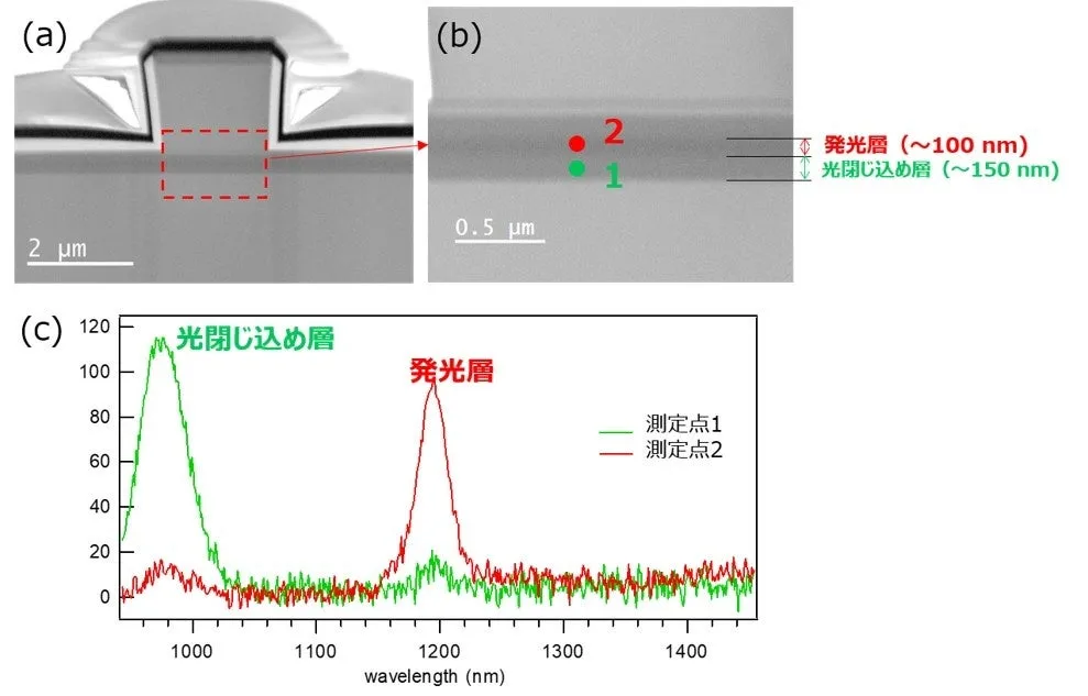
TRC's analytical service has been put to the test in several instances, providing valuable insights into optical components. For example, a commercial near-infrared laser diode evaluation revealed distinct light emission peaks at approximately 1200 nm in the emission layer, confirming the connection to the active layer responsible for laser behavior. Additionally, surrounding layers exhibited different emission characteristics, showcasing the service’s ability to spatially isolate and analyze different functional layers within a device.
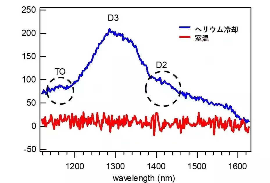
Another example involved assessing crystalline silicon, where low-temperature measurements allowed the observation of weak near-infrared emissions that remain undetectable at room temperature. This ability to evaluate subtle emissions related to crystal defects positions TRC's service as a transformative tool in silicon photonics development, enhancing the understanding of structural changes and their implications on performance.
Conclusion and Future Directions
The introduction of this groundbreaking service reinforces TRC's commitment to advancing analysis techniques pivotal for optical communication and silicon photonics. By continuing to refine and expand these analytical methodologies, including the further sophistication of integrated STEM-CL techniques, TRC aims to facilitate the development of next-generation optical technologies while enhancing the speed and competitiveness of clients' product development processes. In a landscape where speed and efficiency are paramount, TRC’s innovative solutions promise to lead the way toward a more connected future.
The future of optical communication lies not only in faster signals but in a deeper understanding of the devices that transmit them. With TRC's advanced analytical service, the industry is poised to explore unchartered territories in optical device performance and reliability.
Topics Consumer Technology)
【About Using Articles】
You can freely use the title and article content by linking to the page where the article is posted.
※ Images cannot be used.
【About Links】
Links are free to use.