



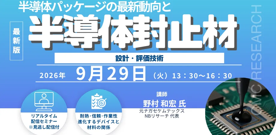
Explore the Latest Trends in Semiconductor Packaging and Material Design Technology: A Live Webinar
Upcoming Live Seminar: Trends in Semiconductor Packaging
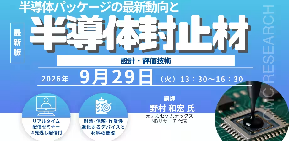
In today's fast-evolving technological landscape, understanding the latest advancements in semiconductor packaging is essential. Join us on September 29, 2026, from 13:30 to 16:30 for a comprehensive live seminar titled "Latest Trends in Semiconductor Packaging and Design and Evaluation Techniques for Sealing Materials." This session is organized by CMC Research Inc..
Seminar Overview
The semiconductor industry plays a pivotal role in various sectors including automotive, healthcare, communications, and artificial intelligence. As the demand for smaller and faster devices rises, innovative packaging designs such as chiplets and 3D packages have been proposed, leading to a diverse set of requirements for sealing materials. This seminar strives to address the evolving needs of sealing materials in the context of contemporary packaging technologies.
What You Will Learn
Participants will delve into the following topics:
- - The latest trends in semiconductor packaging
- - Fundamental raw materials used in sealing materials
- - Design techniques for sealing materials
- - Evaluation techniques for sealing materials
The seminar is designed for a wide range of attendees, including sealing material designers, technicians utilizing sealing materials, and those involved in the design of epoxy resins and hardeners specific to semiconductor applications.
Detailed Agenda
1. Introduction to Semiconductor Packaging
- Types of packages: Wire bond, flip chip, wafer level, and advanced packages
- Molding methods: Transfer molding, compression molding, and printing/dispensers
2. Design of Sealing Materials
- Key materials: Epoxy resins, hardeners, and additives
- Required characteristics and design requirements for sealing materials
- Technologies for reducing stress
3. Evaluation Techniques
- Individual evaluation of sealing materials: Heat resistance, humidity resistance, and purity
- Package-level evaluations: Moisture reflow testing, heat cycle testing, and high-temperature high-humidity tests
4. Next-Generation Sealing Materials
- Low dielectric, high thermal conductivity, and optoelectronic integration technologies
Meet Your Instructor
The seminar will be led by Kazuhiko Nomura, the representative of NB Research. With an extensive background in polymer science and semiconductor sealing materials, he offers expert insights into the intricate world of semiconductor technologies. His experience includes over 30 years in the industry, having worked with leading firms and developed significant innovations in sealing materials and various resin applications.
How to Participate
Registration Fee:
- - General: ¥44,000 (tax included)
- - Newsletter subscribers: ¥39,600 (tax included)
- - Academic: ¥26,400 (tax included)
The seminar will be conducted via Zoom, allowing participants to join from anywhere. If you're unable to attend the live session, a recorded version will be provided for limited playback afterward.
Secure your spot now! Visit here for registration details. And feel free to participate during the Q&A time to gain clarity on your specific queries.
Don’t miss out on this opportunity to enhance your understanding and skills in semiconductor packaging and material design. Join us on September 29, 2026 for an enlightening experience tailored for professionals like you!
Topics Consumer Technology)
【About Using Articles】
You can freely use the title and article content by linking to the page where the article is posted.
※ Images cannot be used.
【About Links】
Links are free to use.