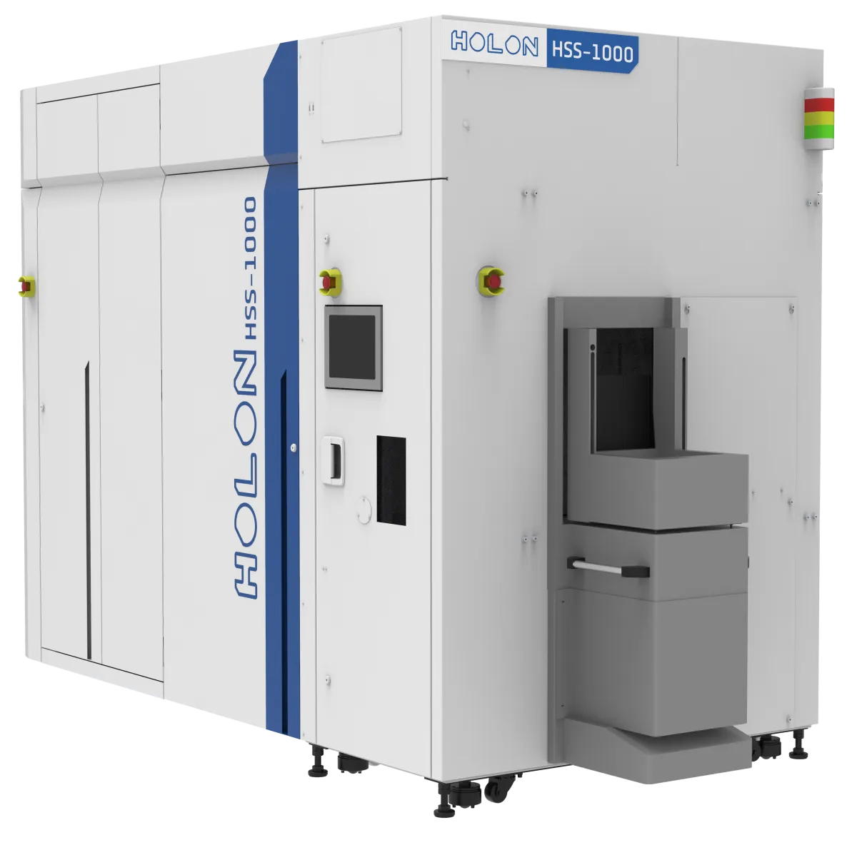
Holon's New HSS-1000 CD-SEM Marks a Breakthrough in Measurement Technology


Holon's Revolutionary HSS-1000 CD-SEM
Holon, a consolidated subsidiary, has launched its new product, the next-generation CD-SEM known as the HSS-1000. This innovative device significantly enhances performance compared to its predecessor, the ZX, achieving unparalleled CD measurement precision required for EUV mask production beyond the 1.6nm node. Moreover, it enables high-resolution SEM imaging of thin film absorption layers and experimental resists, greatly contributing to yield improvement in mass production and efficiency in mask development.
Product Overview
The HSS-1000 utilizes advanced technologies to tackle the challenges posed by the rapid miniaturization of mask patterns due to the full-scale adoption of EUV lithography. Key concerns like improved CD measurement accuracy, ensuring throughput, precisely observing thin film absorption layers and resists, and edge position detection for curved patterns prompted the development of this state-of-the-art instrument. By leveraging our group's innovative technologies, we have produced a solution capable of addressing these industry challenges.
Key Features
1. New Electronic Optical System: The HSS-1000 features a redesign of the electronic optical system and aberration correction technology, enabling remarkably fine SEM images and significantly improving observation precision of intricate patterns.
2. High-Precision Beam Control Circuits: Equipped with beam control circuits that offer precision and speed comparable to drawing devices, the HSS-1000 facilitates rapid and exact CD measurements, enhancing its mass production capabilities.
3. Low-Damage Observation: With a low incident energy of 100 eV, it provides low-damage observation of resists, allowing for high-resolution imaging while controlling resist shrinkage.
4. High Throughput: The new platform's pallet-free transport system and high-speed stage have dramatically increased throughput, meeting the demands of mass production environments.
5. AI Technology for Image Improvement: By using AI, the HSS-1000 delivers predictive corrections for beam focus and position shifts, alongside de-noising processes to further enhance and stabilize SEM images.
6. Strong Charge Mitigation: A combined approach utilizing low vacuum and VUV light minimizes image degradation from charging effects, ensuring stable observations.
7. Accurate Curvilinear Measurement: Thanks to its high-precision contour extraction capabilities, the HSS-1000 can measure edge positions of curved patterns with exceptional accuracy.
Performance Comparison with ZX Model
- - Dimension Measurement Accuracy: Improved by 25%
- - Beam Sharpness: Increased by 15%
- - Contrast to Noise Ratio (CNR): Enhanced by 15%
- - Measurement Time: Reduced by 30%
Future Directions
As part of our ongoing commitment to innovation, our group will strengthen development resources to cater to customer-specific needs with precision. Additionally, we are focused on deepening our foothold in the Asian market while reinforcing our expansion endeavors in Europe and the United States based on the HSS-1000.
About Holon
Holon specializes in leveraging electron beam technology to deliver solutions in the semiconductor and nanotechnology sectors. Utilizing expertise gained from photo mask observation and measurement, the company develops and markets systems for ultra-fine processing in HDD, MEMS, and nanoimprint technologies. For more information, visit Holon Ltd..
For inquiries, contact:
A&D Holon Holdings
Corporate Planning & Public Relations Department
TEL: 03-5391-6124
Topics Consumer Technology)
【About Using Articles】
You can freely use the title and article content by linking to the page where the article is posted.
※ Images cannot be used.
【About Links】
Links are free to use.