



Lintec to Establish New Semiconductor Solutions Lab in Fukuoka by 2028
Lintec Sets Plans for New Semiconductor Solutions Lab in Fukuoka
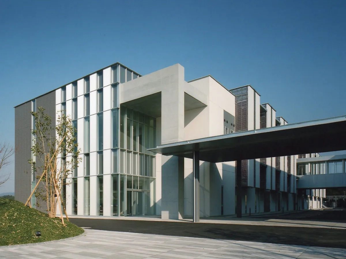
Lintec, headquartered in Itabashi, Tokyo, is embarking on an ambitious project to open a new research facility dedicated to semiconductor technology. This facility, named the Semiconductor Solutions Lab, is set to be constructed in the Itoshima Research Park in Fukuoka Prefecture with an investment of approximately 20 billion yen. The completion is expected in October 2028. This initiative aligns perfectly with the regional economic revitalization efforts of both Fukuoka Prefecture and Itoshima City. To formalize this development, a tripartite location agreement signing ceremony will take place on August 21 at the Fukuoka Prefectural Office.
In recent years, the semiconductor industry has witnessed a surge in demand, especially for applications related to artificial intelligence. As manufacturing technologies undergo significant transformations, the boundaries between initial and final processes in semiconductor production are increasingly blurred. Innovations such as three-dimensional (3D) integration and chiplet technology are gaining prominence, emphasizing the importance of intermediate processes concerning performance, yield, and reliability.
To capitalize on these trends and enhance foundational technologies from a mid- to long-term perspective, Lintec has been strategically developing its capabilities. Previously, the company established the Packaging Technology Development Room within the Fukuoka Super Integration Semiconductor Solutions Center, operated by the Fukuoka Prefectural Industrial and Scientific Technology Promotion Foundation. The establishment of the Semiconductor Solutions Lab will strengthen Lintec's long-term growth strategy amid structural changes in the semiconductor sector.
New Development Hub to Foster Customer Collaboration
The upcoming Semiconductor Solutions Lab will feature a cleanroom environment equipped with various intermediate and final production equipment, along with essential analysis and testing apparatus, sourced from both Lintec and other manufacturers. This development center is positioned as a collaborative and responsive hub for technological advancement, aiming to swiftly address the next generation of semiconductor processes alongside customers.
Lintec has already established application centers in Japan, Taiwan, Malaysia, and North America, focusing on optimizing processing conditions, material evaluation, and process validation. Through tight collaboration with these centers, Lintec intends to fortify its global R&D framework, enhancing the group’s ability to propose comprehensive solutions encompassing materials, equipment, and processes.
Overview of the Semiconductor Solutions Lab
- - Investment Amount: Approximately ¥20 billion
- - Planned Completion: October 2028
- - Location: Higashi, Itoshima City, Fukuoka Prefecture
- - Site Area: 3,435 m²
- - Building Structure: Three stories, total floor area of about 5,000 m²
- - Estimated Staff Count: Around 25 (initially 15)
- - Research Focus: Materials for semiconductor and electronic components manufacturing processes
Lintec's Semiconductor Business Profile
Lintec began its journey in the semiconductor market in 1986 with the development of UV-curable dicing tape. The company has since excelled in producing specialized adhesive tapes used in backend semiconductor manufacturing processes. The unique aspect of Lintec's business lies in its ability to develop both the adhesive tapes and the associated equipment for application and removal. Research and development for the tapes are conducted at facilities in Saitama Prefecture, while equipment is developed at the Ina Technology Center in Northern Saitama.
About the Fukuoka Super Integration Semiconductor Solutions Center
The Fukuoka Super Integration Semiconductor Solutions Center, established in August 2025, is a unified hub supporting the entire process from design and prototype development to evaluation and product commercialization. Equipped with state-of-the-art tools necessary for high-density chip packaging, particularly for 3D integration, this center has been pivotal in advancing semiconductor technology. Lintec’s involvement began in October 2023, when it opened the Packaging Technology Development Room to further propel the development of semiconductor-related products and innovative process technologies.
Contact for Release Information
Lintec Corporation
Public Relations & IR Room
23-23 Honmachi, Itabashi-ku, Tokyo 173-0001
Phone: (03) 5248-7741
Fax: (03) 5248-7754
Company Overview
- - Company Name: Lintec Corporation
- - Headquarters: 23-23 Honmachi, Itabashi-ku, Tokyo 173-0001
- - Founded: October 15, 1934
- - Capital: ¥23,355 million (as of March 31, 2026)
- - Stock Code: 7966 (TSE Prime Market)
- - Website: Lintec Official Website
Topics Consumer Technology)
【About Using Articles】
You can freely use the title and article content by linking to the page where the article is posted.
※ Images cannot be used.
【About Links】
Links are free to use.