


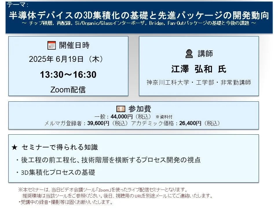
Exploring 3D Integration in Semiconductor Devices and Advanced Packaging Trends
Overview of the Upcoming Webinar
On June 19, 2025, CMC Research will host a comprehensive live webinar dedicated to the topic "Fundamentals of 3D Integration in Semiconductor Devices and Trends in Advanced Packaging Development." The session will be led by Hirokazu Ezawa, a part-time lecturer at Kanagawa Institute of Technology, and will highlight current trends in semiconductor packaging technologies essential for the evolving landscape of AI and other advanced applications.
Key Details of the Webinar
- - Date and Time: June 19, 2025, from 13:30 to 16:30 (JST)
- - Platform: Zoom
- - Registration Fee:
- CMC Newsletter Subscribers: 39,600 JPY (tax included)
- Academic Price: 26,400 JPY (tax included)
- - Speaker: Hirokazu Ezawa, Part-time Lecturer at Kanagawa Institute of Technology
Topics to be Discussed
This seminar will address the transition from 2.5D to 3D integration, focusing on the fundamental processes that underlie these advancements. Attendees will gain insights into:
- - Recent developments in advanced semiconductor device packaging.
- - The progression of intermediate technologies and the enhancement of post-process quality.
- - The foundational principles of 3D integration processes, including device performance improvement strategies such as TSV revisits, wafer-level hybrid bonding, and various integration techniques.
- - An overview of Fan-Out packaging processes and the current market landscape.
Audience Targeted
The webinar is tailored for:
- - Mid-career engineers looking to refresh their foundational knowledge in semiconductor technology.
- - Sales and marketing professionals interested in the trends surrounding advanced semiconductor packages.
- - Representatives from LCD panel manufacturers who are keen on semiconductor packaging.
Why Attend?
As the application of AI continues to grow across various sectors, the demand for high-quality semiconductor packaging techniques is critical not just for enhancing system-level performance, but also for creating a diverse ecosystem that can support timely releases of system modules from a mix of advanced and non-advanced devices. This webinar is an excellent opportunity to deepen your understanding of these technologies and trends.
Webinar Format
The seminar will be delivered live via Zoom, allowing participants to engage directly with the instructor. A Q&A session will follow the presentation, encouraging dialogue and clarification of complex topics.
Registration Details
To secure your spot, please register through the specific webinar page on CMC Research's website. Upon registration, participants will receive an email with a link to join the session before the event date.
Additional Information
Recording of the session for personal use will not be permitted to ensure the integrity of the presented material. More information about this and future webinars, including a comprehensive schedule, can be found on the CMC Research website.
About the Speaker
Hirokazu Ezawa has over 30 years of experience at Toshiba, focusing on Si semiconductor devices and packaging technologies. He now brings his expertise to the academic field while consulting through his own firm, ezCoworks. His involvement with professional societies such as the Japan Society of Materials Science and IEEE showcases his commitment to the continuous advancement of semiconductor technology.
Make sure to not miss this chance to deepen your expertise in semiconductor packaging and integration processes crucial for navigating the future of the electronics market!

Topics Consumer Products & Retail)


【About Using Articles】
You can freely use the title and article content by linking to the page where the article is posted.
※ Images cannot be used.
【About Links】
Links are free to use.