


Canon Marketing Japan to Exhibit at SEMICON Japan 2025 Featuring Advanced Semiconductor Equipment
Canon Marketing Japan to Exhibit at SEMICON Japan 2025
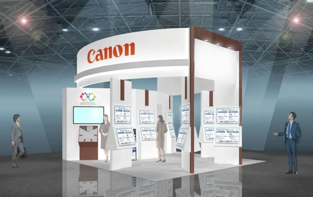
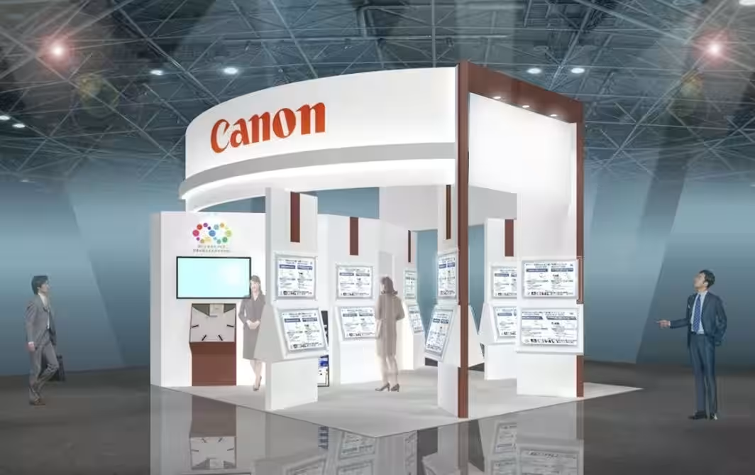
Canon Marketing Japan, also known as Canon MJ, has announced its participation in the upcoming SEMICON Japan 2025 event. This internationally recognized trade show dedicated to the semiconductor industry will be held at Tokyo Big Sight from December 17 to 19, 2025. The company, led by President Masachika Adachi, aims to showcase its extensive range of world-class semiconductor manufacturing equipment alongside innovative technologies that have yet to be introduced in the Japanese market.
A Diverse Portfolio of Manufacturing Equipment
Canon MJ is renowned for its comprehensive service offerings, from sales and installation to troubleshooting, covering all aspects of semiconductor manufacturing equipment. At SEMICON Japan 2025, they plan to present newly added products alongside the most advanced equipment in the industry. This includes a lineup featuring saltwater coating, etching machines, and the latest inspection devices.
Among the highlighted products are the cutting-edge PVA Tepla ultrasonic microscope, high-speed AFM (Atomic Force Microscopy) tools for advanced semiconductors, and measurement devices specifically designed for EUV masks and blanks. Canon MJ will also showcase a wide range of process equipment, such as:
- - 300mm wafer-compatible plasma etching and annealing equipment
- - Wet etchers and CVD (Chemical Vapor Deposition) systems for wafers smaller than 200mm
This expansive offering epitomizes Canon MJ’s commitment to supporting semiconductor manufacturers with the best technology available.
Introduction of Unprecedented Technologies
Another point of emphasis at this year’s exhibition will be the introduction of innovative technologies and equipment that are currently unavailable in Japan’s domestic market. Key players like NANOSEEX and Wooptix will showcase remarkable devices, including a 3D structure inline XRR (X-ray Reflectivity) apparatus and a wafer shape measurement device utilizing a new measurement principle. These introductions are expected to help elevate Japan’s pharmaceutical and technological landscape significantly.
SEMICON Japan 2025 Overview
SEMICON Japan is an annual international exhibition focused exclusively on the semiconductor industry. This event marks the 49th installment and is organized by SEMI, a global industry association committed to fostering the growth of the semiconductor sector. Alongside SEMICON Japan, similar events are held across the globe, including SEMICON Europa, SEMICON West in the United States, and SEMICON China.
The exhibition serves as a valuable platform for attendees to gain insights into market and technology trends in semiconductors, which are integral to groundbreaking fields such as AI, autonomous driving, and high-speed 5G/6G communication. Furthermore, it fosters interactions among engineers and industry professionals through networking opportunities.
Event Details
- - Dates: December 17 (Wednesday) to December 19 (Friday), 2025
- - Hours: 10:00 AM - 5:00 PM
- - Location: Tokyo Big Sight
- - Admission Fee: Free (Pre-registration required)
- - Booth Location: East Exhibition Hall, 1st Floor
For inquiries from the general public about Canon MJ and their showcased devices, please contact:
- - Canon Marketing Japan, Process Equipment Sales Department, Sales Second Division at 03-3740-3315 (Direct Line)
Topics Consumer Products & Retail)


【About Using Articles】
You can freely use the title and article content by linking to the page where the article is posted.
※ Images cannot be used.
【About Links】
Links are free to use.