Latest Trends in Semiconductor Packaging Materials and Design Evaluation Techniques Webinar


Discover the Future of Semiconductor Packaging
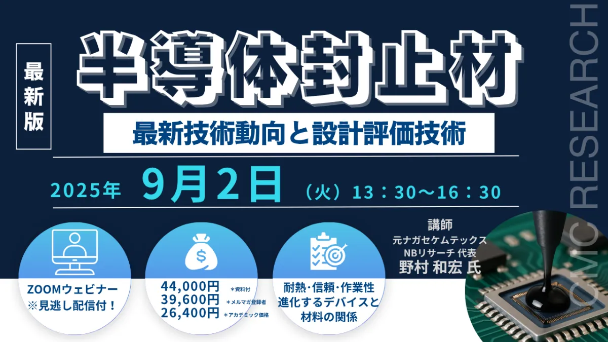
On September 2nd, 2025, CMC Research Inc. will host an enlightening online seminar titled "Latest Trends in Semiconductor Packaging Materials and Design Evaluation Techniques". With the rapid advancements in the semiconductor industry, grasping the latest insights on materials and their design evaluations has become paramount for professionals in the field.
Overview of the Seminar
The seminar will commence at 13:30 and conclude at 16:30, featuring esteemed speaker Kazuhiro Nomura, the representative of NB Research. Participants will have a unique opportunity to understand critical trends in semiconductor packaging, especially as applications like autonomous driving, remote healthcare, and AI continue to evolve, demanding higher efficiency and performance.
Key Knowledge Areas to be Covered:
- - Trends in power devices
- - Developments in semiconductor packaging
- - Design techniques for semiconductor packaging materials
- - Evaluation methods for semiconductor encapsulants
Target Audience
This seminar is designed for:
- - Designers of semiconductor encapsulating materials
- - Engineers involved in the evaluation of semiconductor materials
- - Developers of epoxy resins and hardeners for semiconductor applications
Seminar Agenda
1. Evolution of Semiconductor Packaging
- Transition in package structures
- From large-area devices to chiplets
- Technologies required for 2.1D, 2.5D, and 3D packaging
- Classification of packages from an encapsulating material perspective
2. Encapsulating Resins for Power Devices
- Applications of power devices
- Current trends and market insights
- Requirements for encapsulating resins, such as high thermal resistance and fire retardancy
3. Encapsulating Resins for IC Packaging
- Essential properties like heat and moisture resistance
- Techniques for wire bond encapsulants
- Challenges and requirements for flip chip encapsulants
4. Evaluation Methods for Semiconductor Encapsulants
- Assessing workability and reactivity
- Electrical properties evaluation
- Analysis of moisture absorption and residual stress
Registration and Participation
To participate, register via the CMC Research seminar webpage. A URL for streaming will be emailed following your registration, allowing you to view the seminar live or access a recorded version later. Note that recording or photographing the session is strictly prohibited.
Why Attend?
With the rise of new technologies necessitating innovative approaches within semiconductor materials, this seminar provides essential insights and discussions that could shape your projects and enhance your understanding of market trends. There will also be a Q&A segment to address participant inquiries.
For further details and registration, please visit CMC Research’s official website. Don't miss out on the chance to stay ahead in the fast-paced semiconductor industry!
Topics Consumer Technology)
【About Using Articles】
You can freely use the title and article content by linking to the page where the article is posted.
※ Images cannot be used.
【About Links】
Links are free to use.