Explore Advanced Semiconductor Defect Evaluation Techniques in Upcoming Seminar


Upcoming Seminar on Next-Generation Semiconductor Technologies
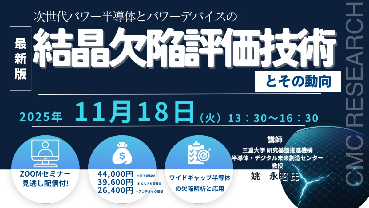
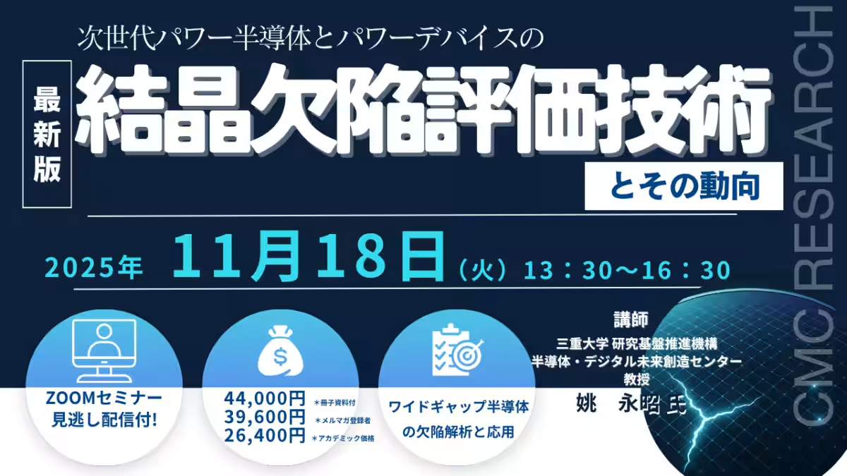
In an era where technology evolves rapidly, the field of semiconductors remains pivotal, particularly regarding the evaluation of defects in semiconductor materials. CMC Research is proud to host a live seminar titled "Techniques and Trends in Crystal Defect Evaluation of Next-Generation Power Semiconductors and Devices" on November 18, 2025, from 1:30 PM to 4:30 PM JST, via Zoom.
Seminar Overview
The seminar will be presented by Professor Yao Yongzhao from Mie University, a leading figure in semiconductor research. Participants can expect an insightful exploration of wide-bandgap semiconductors, including materials like 4H-SiC, GaN, and β-Ga2O3. These materials are known for their superior performance characteristics, such as high power density, low loss, and temperature stability, compared to traditional semiconductors. However, they present unique challenges in crystal growth, leading to the formation of various lattice defects that can significantly affect device performance and reliability.
Attendees will acquire substantial knowledge that will aid in improving the performance and reliability of next-generation power devices, making this seminar a must for researchers and technicians engaged in semiconductor crystal defect evaluation.
Key Learning Outcomes
1. Crystal Structure: Understand the fundamental structures of semiconductor crystals.
2. Types of Defects: Gain insights into various defects present in crystals and their origins.
3. Evaluation Methods: Learn about the techniques to assess these defects efficiently, such as X-ray diffraction and electron microscopy.
4. Impact of Defects on Devices: Explore how these defects influence the electrical characteristics and overall behavior of semiconductor devices.
Target Audience
This seminar is aimed at researchers and engineers working in the field of semiconductor crystal defect evaluation, making it an excellent opportunity to enhance your expertise in this niche area.
Program Schedule
The seminar will cover several essential topics:
1. Introduction to power-device wide-bandgap semiconductors and the types of defects.
2. Crystal Evaluation Techniques: A detailed discussion on methods including selective chemical etching, TEM, and X-ray topography.
3. Device Evaluation: Focus on how defects impact device functionality.
4. Conclusion: Summary and key takeaways.
Participation Fees
- - General: 44,000 yen (including tax)
- - Newsletter subscribers: 39,600 yen (including tax)
- - Academic rate: 26,400 yen (including tax)
To ensure that everyone can benefit from this knowledge, a recorded version will be available for those who cannot attend the live session.
Registration Information
Interested participants can register via the following link: CMC Research Seminar Registration. Once registered, you will receive a URL for attending the seminar via email.
Conclusion
Advanced semiconductor technologies are at the forefront of innovation across multiple industries. This upcoming seminar provides an exceptional platform to delve deeper into the critical aspects of semiconductor defect evaluation with insights from experts. We encourage all relevant professionals to register and enhance their understanding of these vital technologies.
Topics Other)


【About Using Articles】
You can freely use the title and article content by linking to the page where the article is posted.
※ Images cannot be used.
【About Links】
Links are free to use.