




Kaijo's New Ultrasonic Cleaning System for Semiconductor Applications: QUAVA mini Mega Puck
Introduction
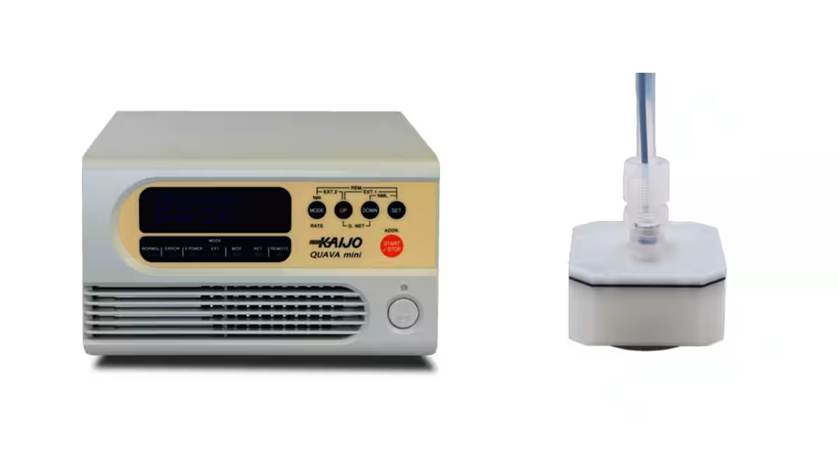
Kaijo Inc., based in Hamura City, Tokyo, has launched an innovative ultrasonic cleaner named the QUAVA mini Mega Puck, targeting precise cleaning for semiconductor manufacturing, specifically for wafers, resist stripping, and residue removal after etching. This new product leverages Kaijo's unique liquid contact cleaning method to create a liquid membrane that effectively removes fine contaminants. Combining high-frequency ultrasonic waves at 3MHz, it achieves ultra-high cleanliness while ensuring damage-free cleaning of delicate circuits.
Development Background
Recent advancements in semiconductor technology have significantly boosted performance and miniaturization. As a result, even minor particle adhesion and residues from resist stripping and etching can precipitate circuit shorts and reduce yield. These conditions necessitate a higher standard of ultra-clean cleaning processes than ever before. However, with the ever-tinier circuit patterns comes a risk: traditional powerful ultrasonic cleaning can damage sensitive circuits (e.g., pattern collapse). To overcome these conflicting demands for thorough cleaning power and damage-free operation, Kaijo harnessed years of ultrasonic technology expertise to innovate and release this state-of-the-art product.
Product Features
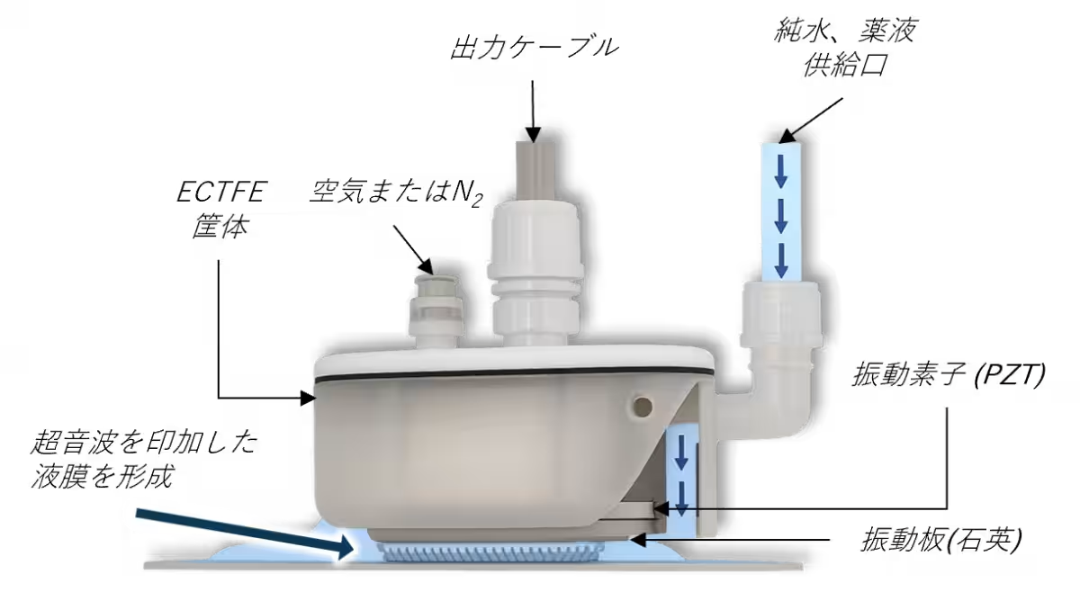
The QUAVA mini Mega Puck is a groundbreaking ultrasonic cleaning system that utilizes Kaijo’s proprietary liquid contact cleaning method. This technique ensures that ultrasonic vibrations are transmitted uniformly, eliminating inconsistent cleaning results across surfaces.
Unique Transducer Design
In high-frequency ultrasonic cleaning, it's critical to maintain an optimal distance between the transducer and the item being cleaned. If this distance is incorrect, ultrasonic energy can dissipate. To address this, the QUAVA mini Mega Puck is equipped with a gap indicator function on its oscillator, which maintains proper distance and ensures stable ultrasonic wave propagation.
Additionally, the system features a range of transducer materials including quartz, stainless steel, and sapphire, allowing it to be compatible with various cleaning agents. The incorporation of a cooling mechanism for the transducer stabilizes frequency and enables prolonged operation, thus extending the life of the components.
Comparison with Other Cleaning Methods
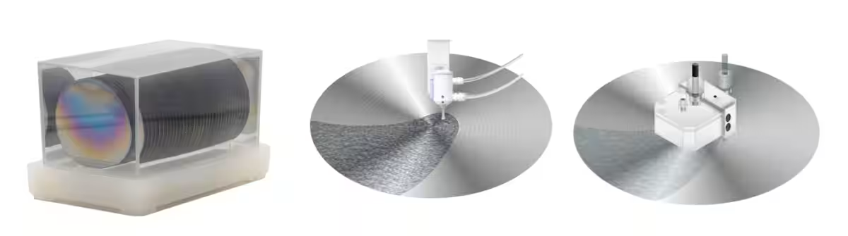
In semiconductor manufacturing, there are three main cleaning methods:
- - Batch Method: Well-suited for large-scale processing but can lead to uneven cleaning and the risk of re-adhesion of removed contaminants.
- - Shower Method: Continuous flow of fresh liquid minimizes re-adhesion risk but lacks uniform coverage and can potentially damage delicate circuits due to centrifugal forces.
- - Liquid Contact Method: Offers broad ultrasonic effective areas, providing uniform ultrasonic application, ensuring no cleaning unevenness, and increasing contact frequency with deep holes even at low rotations.
Recommended Applications and Main Work Items
This product is optimal for sectors with stringent cleanliness and damage-free requirements, particularly:
- - Semiconductor device manufacturers, focusing on front-end processes.
- - Manufacturers of semiconductor production equipment.
- - Producers of electronic components, optical elements, and silicon wafers.
Primary Applications:
- - Advanced Semiconductor Wafers (Silicon, SiC, GaN, etc.): Enables thorough particle removal from the nano to micron scale and ensures the delicate cleaning of wafers at risk of pattern collapse.
- - Resist Stripping and Etching Processes: Enhances ultrasonic stripping and etching, achieving complete removal of minute organic and inorganic residues.
- - Photomasks, MEMS, and Optical Substrates: Essential for the removal of contaminants in ultra-precision flatwork where scratches are intolerable.
Technical Specifications
QUAVA mini Oscillator Specifications
| Model | Max Output | Frequency | Oscillation Mode | Power Supply | Dimensions (mm) | Weight (kg) |
|---|---|---|---|---|---|---|
| - | -- | --- | ---- | -- | --- | ----- |
| 20110(QA-001) | 1W – 50W | 950kHz, 3MHz | PLL, A Mode | AC100V – AC240V, 250VA | 218x258x138 | 5 |
| 20110(QD-027) | 1W – 50W | 950kHz, 3MHz (Dual) | PLL, A Mode | AC100V – AC240V, 250VA | 218x258x138 | 5 |
Mega Puck Transducer Specifications
| Model | Frequency/Input | Housing Material | Diaphragm Material | Liquid Temp. | Liquid Volume | Air Purge Flow | Dimensions (mm) | Weight (kg) |
|---|---|---|---|---|---|---|---|---|
| - | ---- | ---- | ----- | --- | ---- | --- | ---- | --- |
| 28230 | 950kHz/50W | ECTFE | Quartz | 15-40°C | 1.0-2.0L/min | ~10L/min | 65x74x38 | ~0.4 |
| 28231 | 950kHz/50W | ECTFE | Sapphire | 15-40°C | 1.0-2.0L/min | ~10L/min | 65x74x38 | ~0.4 |
Company Overview
Kaijo has built its reputation on advanced ultrasonic technology, specializing in the development, manufacturing, and sales of semiconductor production equipment and ultrasonic cleaning devices. The company is flexible in customizing transducers, cleaning tanks, and diaphragms according to customer needs.
Founded from the vision of applying acoustic measurement technology from wartime to contribute positively to post-war recovery, Kaijo launched its first ultrasonic cleaner, the Sonocleaner, in 1958, which received considerable attention. Since then, the company has focused not just on emitting ultrasonic waves but also on rigorous component cleaning experiments and evaluations, ensuring the design and manufacturing of high-quality products for over 70 years as a pioneering trusted brand in the state-of-the-art semiconductor industry.
For inquiries regarding this product, please contact:
Kaijo Inc. Ultrasonic Equipment Division
Phone: 042-555-6456
Fax: 042-555-0291
Address: 3-1-5 Sakaemachi, Hamura City, Tokyo, 205-8607, Japan
Website: www.kaijo.co.jp

Topics Consumer Technology)
【About Using Articles】
You can freely use the title and article content by linking to the page where the article is posted.
※ Images cannot be used.
【About Links】
Links are free to use.