


Breakthrough in Silicon Photonics: Microscopic Optical Monitor Amplifies Photocurrent by 340 Times
Introduction
In a remarkable advancement in silicon photonics, researchers at Waseda University have developed a groundbreaking microscopic optical monitor. This device can amplify photocurrent by an impressive 340-fold, significantly enhancing the precision of optical circuits used in AI data centers and LiDAR systems.
Key Features of the Development
This novel monitor utilizes a multi-mode interference structure that dramatically improves sensitivity while maintaining low loss, achieving critical breakthroughs that could revolutionize the field.
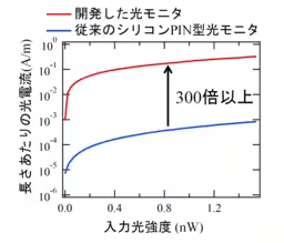
- - High Sensitivity: The monitor demonstrated detection sensitivity approximately 340 times greater than conventional silicon PIN-type detectors.
- - Low Loss Operation: With minimal optical loss and a device size of just a few micrometers, it combines performance and compactness efficiently.
- - Simple Structure: Constructed solely from silicon, the monitor operates without the need for complex materials or amplifiers, ensuring low power consumption.
This development addresses the growing need for reliable operation and power savings in large-scale optical communication circuits, especially as the adoption of generative AI continues to expand.
Rationale Behind the Research
In recent years, generative AI's rapid proliferation has prompted substantial data processing demands within AI data centers. Optical communication is increasingly favored due to its ability to transmit vast amounts of information swiftly and efficiently, replacing traditional electrical wiring. Additionally, high-precision optical control technologies are crucial in applications like LiDAR, which rely on accurate distance and shape measurements.
In silicon photonics, various structures, such as ring resonators and interference circuits, are utilized to manage light effectively. However, these circuits are vulnerable to environmental changes and manufacturing variances that could impair performance. Thus, precise monitoring and control of light intensity and resonant states are essential, especially as circuits scale.
Achievements of the Research
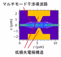
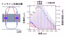
The newly developed inline optical monitor is designed for direct integration into silicon photonic circuits. By leveraging multi-mode interference within silicon waveguides, the researchers successfully minimized optical losses while maximizing sensitivity.
Focusing on the interaction of light in these waveguides, they strategically positioned electrodes at points where the optical field concentration peaks occur. This innovative design drastically reduces the distance between electrodes to enhance photoconductive gain, thereby augmenting the photocurrent without compromising the optical transmission integrity.
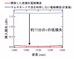
The final inline optical monitor measures just 4.7 micrometers in length and achieves an insertion loss of around 0.03 dB, which is an unprecedented low in comparison to traditional setups—equaling about 1/75 reduction in loss. This efficiency translates into a broader wavelength operation range applicable for both communication and sensing applications. Notably, this monitor records approximately 340 times more sensitivity than existing silicon-PIN detectors by amplifying generated charge rather than merely increasing optical absorption.
Future Implications and Societal Impact
The implications of this breakthrough are far-reaching. As data centers continue to grow in complexity and size, ensuring efficient and stable optical communication remains paramount. This innovative monitor not only meets these demands but also aligns with the evolving landscape of Co-Packaged Optics, which aims to enhance data transmission further and reduce power consumption across communication networks.
Furthermore, the monitor's low-loss attributes make it suitable for integration with LiDAR systems, where precise monitoring of optical intensity and resonance states is essential. Its straightforward silicon construction offers compatibility with existing manufacturing processes, promising cost-effectiveness and feasibility for mass production.
Looking Ahead
In the future, the integration of this monitor into larger silicon photonics systems will be explored, specifically focusing on multi-wavelength optical transceivers for data center interconnects. The ultimate goal involves real-time monitoring of optical intensity and dynamic optimization within these circuits.
Also, advancements in LiDAR applications are on the horizon, where pairing this monitor with technologies like ring resonators will enhance optical beam control's precision and stability. This innovation may also extend to THz wave coherent communication systems, supporting rapid advancements in optical modulation and source stability.
The impetus behind this research emphasizes the critical need for high-precision monitoring technologies in scalable and multifunctional silicon photonics. By successfully bridging the gap between high sensitivity and low-loss operation with a simplified structure, this study lays the groundwork for future exploration across various domains, heralding a new era in photonics that synergizes communication and sensing technologies.

Topics Consumer Technology)
【About Using Articles】
You can freely use the title and article content by linking to the page where the article is posted.
※ Images cannot be used.
【About Links】
Links are free to use.