New Sensitizing Dry Film 'Sunfort™' Developed for Advanced Semiconductor Packaging


New Sensitizing Dry Film 'Sunfort™' Developed for Advanced Semiconductor Packaging
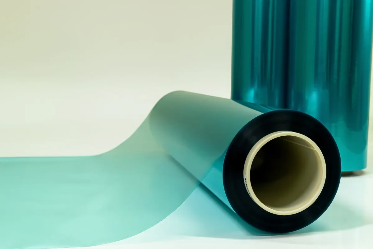
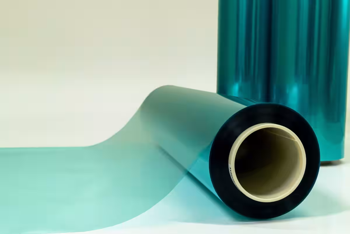
In May 2025, Asahi Kasei Corporation, headquartered in Chiyoda, Tokyo, unveiled its cutting-edge photosensitive dry film, the 'Sunfort TA Series', designed specifically for the manufacturing processes of advanced semiconductor packages, including those used in AI servers.
The 'TA Series' is a core product within the company's Electronics sector, a strategic focus in their 'Mid-term Management Plan 2027 - Trailblaze Together'. This innovative film was developed in response to the burgeoning next-generation semiconductor packaging market, which demands increasingly sophisticated manufacturing techniques.
One of the standout features of the 'TA Series' is its compatibility with both traditional Stepper exposure systems and the newer Laser Direct Imaging (LDI) technology. This dual compatibility allows for remarkable resolution, effectively enhancing the ability to form intricate circuit patterns on substrates during the packaging process.
The demand for higher density and complexity in interposers and package substrates used in advanced semiconductor packages has dramatically increased. Complex wiring technologies are now essential, given the trend toward larger sizes and multilayer constructions. Historically, liquid resists have dominated as the go-to materials for forming these fine wiring layers (re-distribution layers or RDL) due to their superior resolution.
However, despite the advantages of photosensitive dry films, such as panel adaptability, ease of handling, and simultaneous processing capabilities on both sides of a substrate, their resolution limitations have prevented them from being used effectively for RDL applications. The new 'TA Series' addresses these challenges, thanks to the advanced materials design and the photomaterial technologies that Asahi Kasei has refined over the years.
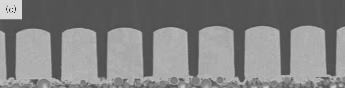
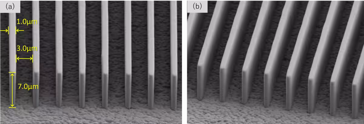
With a targeted design pitch of 4µm for RDL formation, the 'TA Series' demonstrates the capability to overcome prior limitations. It achieves a resist width of 1.0µm patterns using LDI exposure, making it ideally suited for intricate wiring projects, including panel-level packaging. This innovative photosensitive film allows manufacturers to create patterns of 3µm widths through the subsequent processes of plating and resist stripping, expanding the viable applications for high-performance semiconductor packaging.
Moreover, the 'TA Series' supports traditional Stepper exposure methods, providing manufacturers with additional versatility in their fine wiring processes. As technology advances and the demand for larger panel sizes increases, the relevance of panel-level packaging techniques continues to grow, and Asahi Kasei is committed to playing a crucial role in this domain.
In summary, the introduction of the 'Sunfort TA Series' marks a significant advancement in the realm of semiconductor packaging, enabling enhanced resolution and processing efficiency. Asahi Kasei's ongoing innovation in photosensitive dry films will undoubtedly contribute to the future of electronics manufacturing, ensuring they remain at the forefront of this rapidly evolving industry.
For further details, visit the Sunfort™ homepage.
Topics Consumer Technology)
【About Using Articles】
You can freely use the title and article content by linking to the page where the article is posted.
※ Images cannot be used.
【About Links】
Links are free to use.