



KTS Launches EcoTraceDX™ for Non-Destructive PCB Inspection Services
KTS Introduces New Non-Destructive Service for PCB Inspection
In response to the urgent need to manage low-concentration PCB waste, Kanto Tech Solutions (KTS) is set to launch its new service, EcoTraceDX™ for PCB. Effective from August 17, 2026, this service addresses the difficulties in identifying PCB content, especially in equipment with missing nameplates or ambiguous models. This initiative comes amid the approaching deadline for dealing with low-concentration PCB waste, which is mandated to be disposed of by March 31, 2027.
As the Japanese government calls for comprehensive inspections of electrical equipment remaining in facilities, many challenges arise in the field. Equipment is often discovered that cannot easily be categorized, such as those with unreadable nameplates, unknown models, or past documentation that is no longer available. Particularly troubling are devices for which it is not clear whether they contain PCB, making their safe disposal a pressing matter.
KTS recognizes the importance of EcoTraceDX™ for PCB to support customers in the safe disposal of equipment that may contain unknown substances. By examining the internal structure of these devices without causing any damage, KTS provides a vital assessment tool by confirming the presence and placement of components like capacitors.
Using X-ray Technology for Internal Structure Visualization
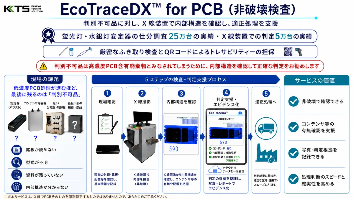
The EcoTraceDX™ for PCB service employs X-ray technology to non-destructively inspect the internal components of electrical devices. The imaging reveals critical details about the device’s internal wiring, windings, cores, and circuit boards that are not visible externally. It’s key to note that while this service does not directly measure the levels of PCB, it allows for an informed judgment regarding the potential for PCB presence based on internal component analysis.
KTS has previously accumulated valuable experience over the past nine years, investigating over 250,000 devices, predominantly fluorescent light fixtures and mercury lamps. Their service has yielded an extensive record of X-ray assessments on more than 50,000 devices, showcasing their expertise in accurately identifying PCB-related risks. Recently, KTS has completed inspections of various unidentified items from older research facilities, large manufacturing sites, and public works, ensuring appropriate evaluation and handling.
Comprehensive Support from Inspection to Regulatory Consultation
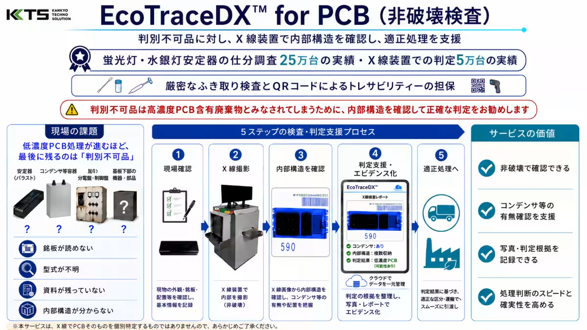
The structured process of the EcoTraceDX™ for PCB service comprises several core steps:
1. Physical Inspection: Assessment of the equipment’s exterior, nameplate, model, and wiring.
2. X-ray Imaging: Non-destructive internal scanning via advanced X-ray devices.
3. Structural Assessment: Evaluation of X-ray images to identify and locate essential components like capacitors.
4. Support and Documentation: Compilation of images, X-ray data, and findings to develop a clear basis for judgement.
5. Proper Disposal and Regulatory Support: Formulation of a disposal strategy based on findings, including consultations with relevant authorities when necessary.
To enhance tracking and compliance, each surveyed item will be affixed with a QR code connecting it to its inspection data. This will allow clients to trace the inspection history effectively. As the deadline for low-concentration PCB disposal approaches, KTS is committed to ensuring that no device is left unassessed, especially since the most challenging items tend to resurface as inspections progress.
KTS emphasizes the importance of not merely retaining equipment out of uncertainty or hastily deciding on disposal methods without thorough inspection. Its philosophy revolves around gaining insight into device internals, documenting findings, and ensuring responsible disposal methods based on well-founded evidence.
Whether it’s uncovering old machines from storage, finding unidentified devices during demolition, or navigating municipal consultation processes, KTS is ready to assist. Any companies struggling with PCB identification issues are encouraged to reach out to KTS for expert guidance.
For more information on the service or to apply, visit the EcoTraceDX website.
About Kanto Tech Solutions
Founded in Chiyoda, Tokyo, Kanto Tech Solutions specializes in various environmental assessments, including PCB and asbestos investigations as well as environmental consulting services. Under the leadership of President Masakazu Shirai, KTS remains dedicated to environmental compliance and innovative solutions in an ever-evolving landscape.
To learn more about KTS, visit our website at KTSOL or reach out via email at [email protected]. EcoTraceDX is a registered trademark of Kanto Tech Solutions.
Topics Environment)
【About Using Articles】
You can freely use the title and article content by linking to the page where the article is posted.
※ Images cannot be used.
【About Links】
Links are free to use.