
Understanding Semiconductor Packaging: Key Concepts and Trends for Quality Management


Seminar on Semiconductor Packaging Fundamentals and Quality Management
Overview
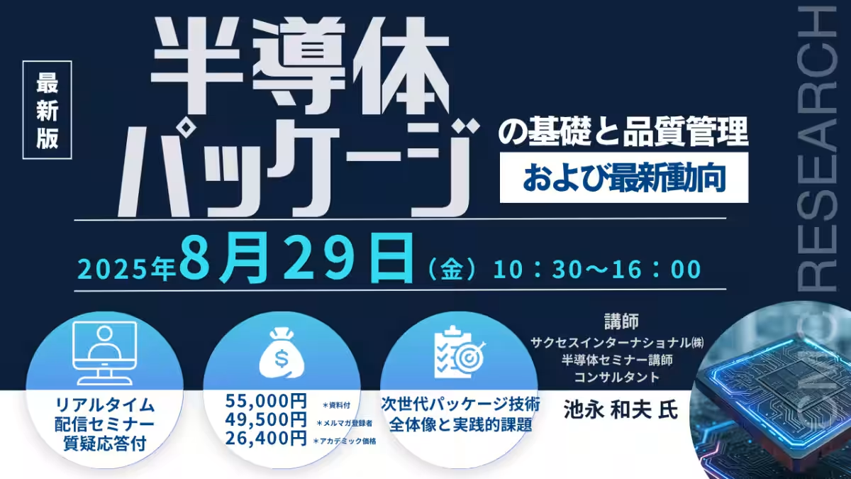
The rapid evolution of technology in the semiconductor industry demands continuous learning and adaptation. To meet this need, CMC Research Co., Ltd., a prominent provider of cutting-edge technology information and market insights, is set to host a seminar titled "Understanding Semiconductor Packaging: Fundamentals and Quality Management" on August 29, 2025. This event will be conducted online via Zoom, starting at 10:30 AM and concluding at 4:00 PM.
Seminar Details
Participants will benefit from the insights of Kazuo Ikegawa, a renowned consultant and seminar instructor from Success International Inc., who will guide the discussions on the latest trends and effective quality management practices in semiconductor packaging. The participation fee is structured as follows:
- - General Admission: ¥55,000 (tax included)
- - CMC Newsletter Subscribers: ¥49,500 (tax included)
- - Academic Rate: ¥26,400 (tax included, materials included)
For more details on the seminar and to register, please visit CMC Research’s website.
Knowledge Participants Will Gain
Attendees will gain a comprehensive understanding of the functional requirements for packaging, the evolution of packaging technologies, and essential quality management practices. This knowledge will deepen insights into the significance of package shape and process interrelations, thereby facilitating future developments in packaging, materials, and equipment.
Furthermore, participants will become equipped to handle contemporary challenges in packaging technologies, preparing them for contributions to future innovations in the semiconductor sector.
Target Audience
This seminar is tailored for:
- - Young engineers specializing in packaging technology
- - Technical and sales representatives from equipment and material manufacturers
- - Anyone enthusiastic about acquiring semiconductor-related knowledge
Seminar Agenda
1. Introduction to Semiconductor Packaging
1. Functionality Requirements of Packaging
2. Historical Evolution and Variety of Packaging
3. Structure and Connection Techniques of Packaging
2. Key Characteristics and Challenges of Assembly Processes (Post-Process)
1. Back Grinding Processes
2. Dicing Processes
3. Die Bonding Techniques
4. Wire Bonding Techniques
5. Mold Packaging Procedures
6. Trimming & Forming Processes
7. Marking Processes
8. Measurement Steps
9. Packaging Processes
3. Quality Standards in Packaging
4. Trends and Challenges in Packaging Technology
1. Electrical Characteristics and Multi-Pin Packages
2. Wafer Level Packaging (WLP)
3. Fan-Out Wafer Level Packaging (FOWLP)
4. System in Package (SiP)
5. Through Silicon Via (TSV)
6. Chiplet and 3D Packaging Trends
5. Conclusion
Presenter Profile
Kazuo Ikegawa
Kazuo Ikegawa serves as a lecturer and consultant for the semiconductor seminars at Success International Inc. His extensive background includes involvement in semiconductor packaging development and production for Sony Corporation, where he held various leadership roles. Following his tenure at Sony, he joined Success International Inc. and has been dedicating his expertise to educating professionals about semiconductor packaging technologies.
Additional Information
This is a live seminar facilitated via Zoom, and participants are encouraged to ensure they meet the recommended technical requirements for the online platform. A URL will be sent post-registration for access to the seminar. Please note that recording or photographing the session is prohibited.
Registration Process
Interested participants are invited to enroll via the official seminar page on the CMC Research website. After registration, a confirmation email with viewing instructions will be dispatched accordingly.
>> Be prepared to immerse yourself in a transformative learning experience that not only enhances your understanding of semiconductor packaging but also enriches your professional network and knowledge base!
Topics Business Technology)
【About Using Articles】
You can freely use the title and article content by linking to the page where the article is posted.
※ Images cannot be used.
【About Links】
Links are free to use.