


Join the Upcoming Seminar on Semiconductor Packaging Technology Fundamentals and Trends
Explore the World of Semiconductor Packaging Technology
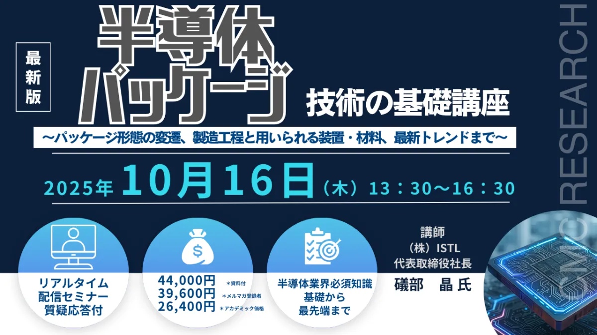
As technology continues to advance, the demand for innovative semiconductor packaging solutions has also grown. On October 16, 2025, CMC Research will host a live seminar titled “Fundamentals of Semiconductor Packaging Technology—Evolution of Packaging Forms, Manufacturing Processes, and Materials Used, along with Latest Trends.” This unique opportunity features a presentation by Akira Isoabe, President of ISTL, who will guide attendees through the intricacies of this essential field.
Seminar Details
- - Date & Time: October 16, 2025, from 1:30 PM to 4:30 PM (JST)
- - Platform: Zoom (Participants will receive materials)
- - Fees:
- Newsletter Subscribers: ¥39,600 (tax included)
- Academic: ¥26,400 (tax included)
The seminar aims to provide foundational knowledge of semiconductor packaging technology, catering to engineers, sales staff, and marketers interested in this field. Attendees will gain critical insights into:
1. The history and evolution of semiconductor packaging technology
2. The manufacturing processes, materials, and equipment involved in packaging
3. Cutting-edge packaging technologies and future directions
Understanding the Notable Shift in Packaging Technology
With the limitations of Moore's Law, it has become increasingly challenging to enhance device performance through advancements in front-end processes alone. Consequently, the evolution of packaging technology is accelerating. This seminar will delve into the evolution of packaging methodologies, explaining them in an accessible manner for beginners, while also discussing the latest advancements in the industry.
Seminar Outline
1. Role of Semiconductor Packaging
1.1 Evolution of Front-end and Back-end Processes
1.2 Changes in Board Assembly Methods
1.3 Requirements for Semiconductor Packaging
2. Changes and Key Technologies in Semiconductor Packaging
2.1 Evolution of PCs and Mobile Phones and Changes in Packaging Forms
2.2 STRJ Packaging Roadmap
2.3 Overview of Various Packaging Types (DIP, QFP, TCP, BGA, WLCSP)
2.4 Key Technologies for Packaging Production (Back Grinding, Dicing, Die Bonding, Wire Bonding, Molding, Bump Technology)
3. Latest Packaging Technologies and Future Directions
3.1 Background Necessitating Advanced Packaging—Limits of Moore's Law
3.2 Overview of Various System-in-Package (SiP)
3.3 What is Fan-out Wafer Level Packaging (FOWLP)?
3.4 What is Chip-on-Wafer-on-Substrate (CoWoS)?
3.5 Understanding Chiplets and Embedded Multi-die Interconnections (EMIB)
3.6 Optical-Electronic Hybrid Packaging
3.7 Future Trends in Packaging Technology
Expert Speaker
Akira Isoabe is an esteemed figure in semiconductor process technology, with a history of leading roles in various prestigious companies, including NEC Corporation and Tokyo Seimitsu. He founded ISTL in 2015 and holds a doctorate in engineering. Isoabe is dedicated to advancing knowledge in the field and is an active member of several academic societies.
How to Participate
Interested individuals can register via the CMC Research seminar site. After registration, a unique Zoom link will be sent via email, enabling you to join the live seminar. Note that all recording and photography during the session are strictly prohibited.
Don't miss your chance to enhance your understanding of this vital area. Join us on October 16, 2025, for an informative session that promises to elevate your knowledge in semiconductor packaging technology!
Topics Other)
【About Using Articles】
You can freely use the title and article content by linking to the page where the article is posted.
※ Images cannot be used.
【About Links】
Links are free to use.