


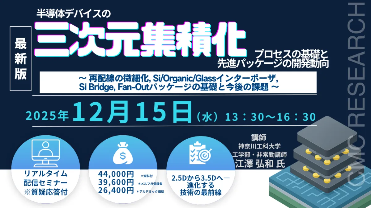
Exploring the Fundamentals and Trends of Advanced 3D Semiconductor Packaging Process Seminar
Upcoming Live Seminar on 3D Semiconductor Processes
Attention all technology enthusiasts and professionals! CMCR Research is excited to announce an engaging live stream seminar titled ‘Fundamentals of 3D Integration Process for Semiconductor Devices and Trends in Advanced Packaging Development’, featuring renowned guest speaker Prof. Hirokazu Ezawa from Kanagawa Institute of Technology. This seminar is scheduled for December 15, 2025, from 13:30 to 16:30 JST and will be conducted on the Zoom platform.
Key Details of the Seminar
In this comprehensive seminar, participants will dive deep into the intricate world of semiconductor technology, exploring the 3D integration process along with recent advancements in packaging technologies. The focus will encompass critical topics such as:
- - Fine Rewiring
- - Si/Organic/Glass Interposers
- - Si Bridge
- - Fan-Out Packages
The discussion will guide attendees from the basics of 3D integration processes to complex concepts like Chiplet integration and the implications for the AI era.
Essential Information
- - Date and Time: December 15, 2025, 13:30 - 16:30 JST
- - Format: Live Zoom Seminar (with materials included)
- - Registration Fees:
- Newsletter Subscribers: ¥39,600 (tax included)
- Academic Pricing: ¥26,400 (tax included)
For registration, please click here.
Why Attend?
This seminar is tailored for:
- - Mid-career engineers seeking a refresher on foundational concepts in semiconductor technology.
- - Sales and marketing professionals interested in the trends of advanced semiconductor packaging.
- - Individuals from LCD panel-related companies wanting to understand semiconductor packaging better.
What Will You Learn?
Participants will gain invaluable insights into:
- - Process development perspectives spanning upstream and downstream engineering components.
- - Basic understanding of 3D integration processes and significant technologies supporting advanced packaging, such as TSV, Hybrid Bonding, and RDL.
Seminar Agenda
The seminar’s structured program will include:
1. Recent advances in advanced semiconductor device packaging:
- CoWoS and Wafer Scale Integration
- Chiplet integration
2. Progress in intermediate technologies and quality enhancements of downstream processes.
3. Fundamentals of 3D integration processes:
- Device performance improvements with TSV re-examination (HBM, BSPDN)
- Wafer Level Hybrid Bonding (CIS, NAND)
4. System-level performance improvements through:
- Logic-on-memory stacked SoC revisión
- 2.5D integration on Si/Organic interposers
5. Basics of Fan-Out (FO) packaging processes.
6. Future development and market trends in the semiconductor packaging sector.
7. Q&A session to clarify concepts discussed during the seminar.
Speaker Profile
Prof. Hirokazu Ezawa has over 30 years of expertise in the microfabrication processes of Si semiconductor devices, marking a significant legacy in both production technology development and academic contributions since 2018 at Kanagawa Institute of Technology. His insight is invaluable for current and future trends in semiconductor packaging.
We encourage professionals and tech-savvy individuals to participate in this significant event to edge ahead in understanding the complexities of 3D semiconductor integration and the evolving landscapes of packaging technologies.
Don’t miss this opportunity to deepen your knowledge and connect with industry experts! For more details and registration, visit the CMCR Research website at https://cmcre.com.
Conclusion
Join us on December 15, 2025, for an informative and engaging seminar that promises to elevate your understanding of semiconductor devices and packaging processes. We look forward to seeing you there!
Topics Other)

【About Using Articles】
You can freely use the title and article content by linking to the page where the article is posted.
※ Images cannot be used.
【About Links】
Links are free to use.