


International Standardization of SiC Power Semiconductors Supported by Defect Testing Enhances Decarbonization Efforts
Enhancing Decarbonization Through SiC Power Semiconductors
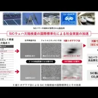
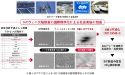
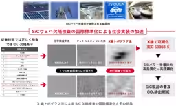
In recent developments, international standards governing the testing of defects in Silicon Carbide (SiC) power semiconductor wafers have been established, particularly the IEC 63068-5 standard. This standard, which employs X-ray topography methods, has been developed to identify and evaluate defects in SiC epitaxial wafers effectively. Given the increasing demand for high-efficiency power loss reduction technologies, especially in electric vehicles and renewable energy sectors, this initiative is a significant leap towards optimizing SiC power devices that are vital for a decarbonized society.
International Standards and Their Importance
Traditionally, the absence of a globally recognized quality evaluation standard for SiC wafers has resulted in variations in product reliability and quality assurance challenges. Recognizing this issue, various academic, governmental, and industrial organizations, such as the National Institute of Advanced Industrial Science and Technology (AIST) and the Japan Electronics and Information Technology Industries Association (JEITA), collaborated to develop a comprehensive quality assessment mechanism over the years. The newly issued IEC standard addresses this gap, focusing on the visualization of crystalline defects—considered as potential production yield and reliability destroyers—that are often overlooked by conventional testing methods.
The introduction of the X-ray topography method enables an extensive examination of SiC crystal structures, significantly improving the precision of defect detection in the wafers. Historically, defects leading to unreliable device performance have been elusive, with detection methods focusing primarily on surface-level inspection. The integration of advanced imaging through X-ray topography helps recognize deeper structural issues, paving the way for enhanced yield rates and overall device reliability.
Addressing Societal Challenges
The mounting urgency for a transition to a decarbonized society accelerates the demand for SiC power semiconductors, which are recognized for their superior efficiency and reliability in electrical systems. The international standardization of evaluation methods, especially involving non-destructive practices like X-ray topography, solidifies the foundation for higher quality assurance in SiC power devices. Previous methodologies, including optical inspections and photoluminescence methods, have facilitated improved quality assessments and social implementations for SiC epitaxial wafers. However, these methodologies struggled against the device-killer defects, necessitating the need for more robust testing frameworks.
The consistency achieved through standardized assessment can lead to reduced quality variations, higher manufacturing yields, and enhanced reliability, thus making SiC devices more dependable for widespread applications in electric vehicles and power infrastructures.
The Path to Standardization
The road to establishing these new standards was paved through continuous effort and research focused on the correlation between crystal defects and device reliability. Initiated around 2001, research into the detrimental impacts of these crystalline imperfections has drawn on collaborative efforts among various stakeholders in academia and industry. Despite the challenges posed by different defect definitions and testing methods across institutions, efforts to establish a unified framework gained momentum through the governmental support provided by projects like the NEDO initiative.
As a result, a series of related standards have emerged since 2019, culminating in the current IEC 63068-5 standard, which addresses the essential identification and evaluation methods necessary for maintaining global competitiveness in the semiconductor market.
Future Directions and Impact
Moving forward, manufacturers of SiC wafers and devices are expected to adopt the newly established IEC standards, enhancing their ability to visualize wafer quality in conjunction with defect identification. This shift promises a substantial reduction in batch variations, improved output rates, and greater trust in SiC power devices, all of which are crucial for the cost-effective expansion into the electric vehicle market and other renewable energy applications.
In the power infrastructure sector, where high-voltage devices are critical, the standardization and subsequent improvement in wafer quality are indispensable for fostering safety and stability. By laying an international groundwork for quality assessment, Japan's advanced techniques can contribute towards elevating trust in its SiC products, bolstering international market presence and reinforcing Japan's semiconductor industry as a robust pillar of economic security.
By promoting research collaborations and supportive scholarly dissemination, a solid standardization process will further the establishment of a reliable framework for SiC wafer quality evaluation and thus drive forward the critical advancements in high-performance and reliable power devices necessary for sustainable technological progression.
Topics Consumer Technology)


【About Using Articles】
You can freely use the title and article content by linking to the page where the article is posted.
※ Images cannot be used.
【About Links】
Links are free to use.