Canon Unveils Innovative Wafer Planarization Technology for Advanced Semiconductor Manufacturing


Canon's Innovative Wafer Planarization Technology
In an impressive leap forward for semiconductor manufacturing, Canon has pioneered a new wafer planarization technology, known as "Inkjet-based Adaptive Planarization" (IAP). This groundbreaking application of Nanoimprint Lithography (NIL) technology marks the world's first practical implementation in the field, aiming for commercialization by 2027.
The Importance of Wafer Planarization
Planarization is a crucial process in semiconductor production, used to ensure a uniform surface on wafers after layers like film deposition and wiring are added. In advanced semiconductors, which are continually evolving with trends toward miniaturization and 3D architecture, even the slightest imperfections in the wafer surface can lead to critical issues such as critical dimension (CD) errors and misalignment of pattern edges. These factors significantly impact yield and overall production efficiency, necessitating more precise planarization techniques than ever before.
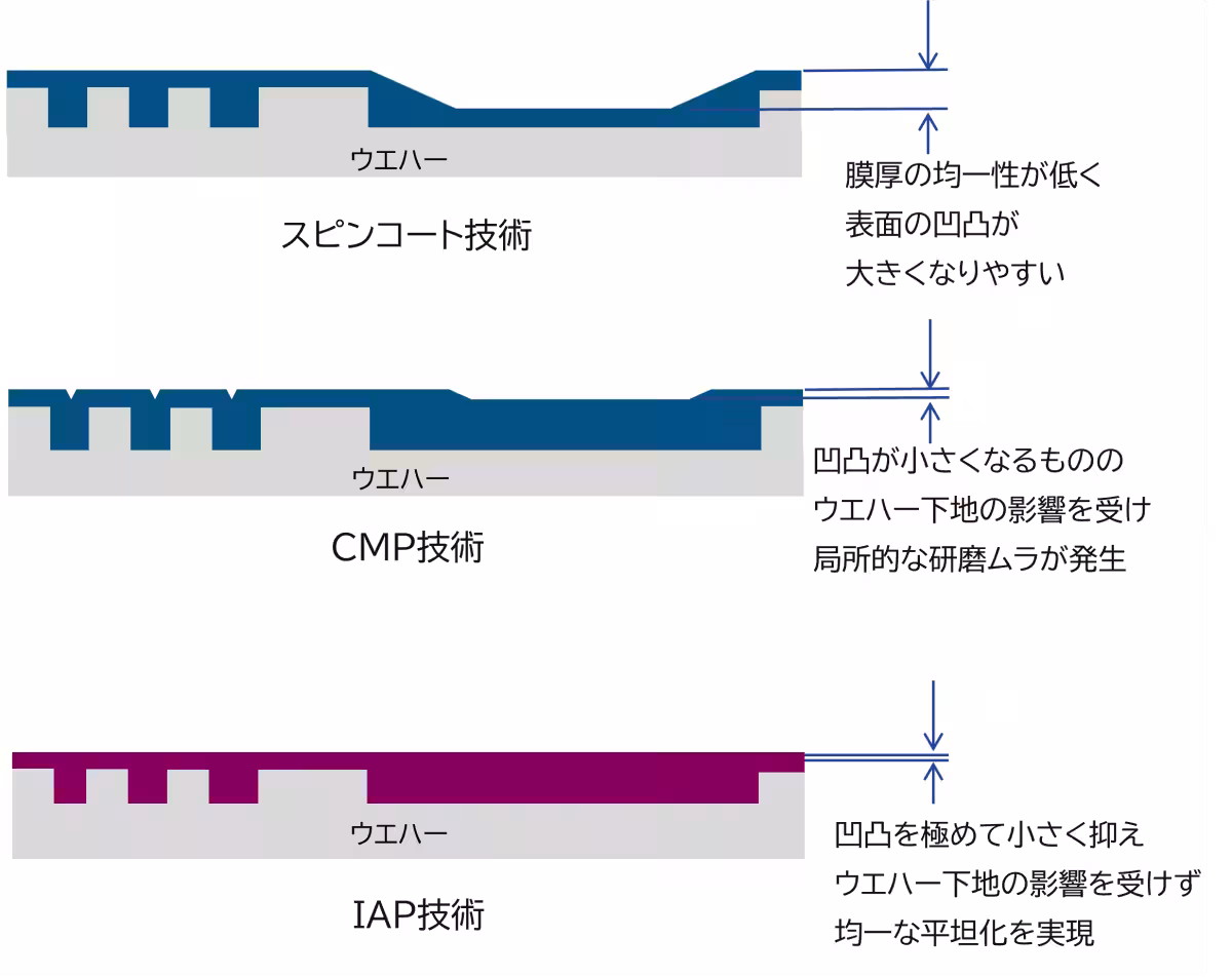
Current prevalent methods include spin-coating that smoothens surfaces by forming thin films and the repetitive chemical mechanical polishing (CMP) technique. However, these methods face challenges related to process complexity and rising costs, which Canon aims to address with its innovative approach.
Canon's Revolutionary IAP Technology
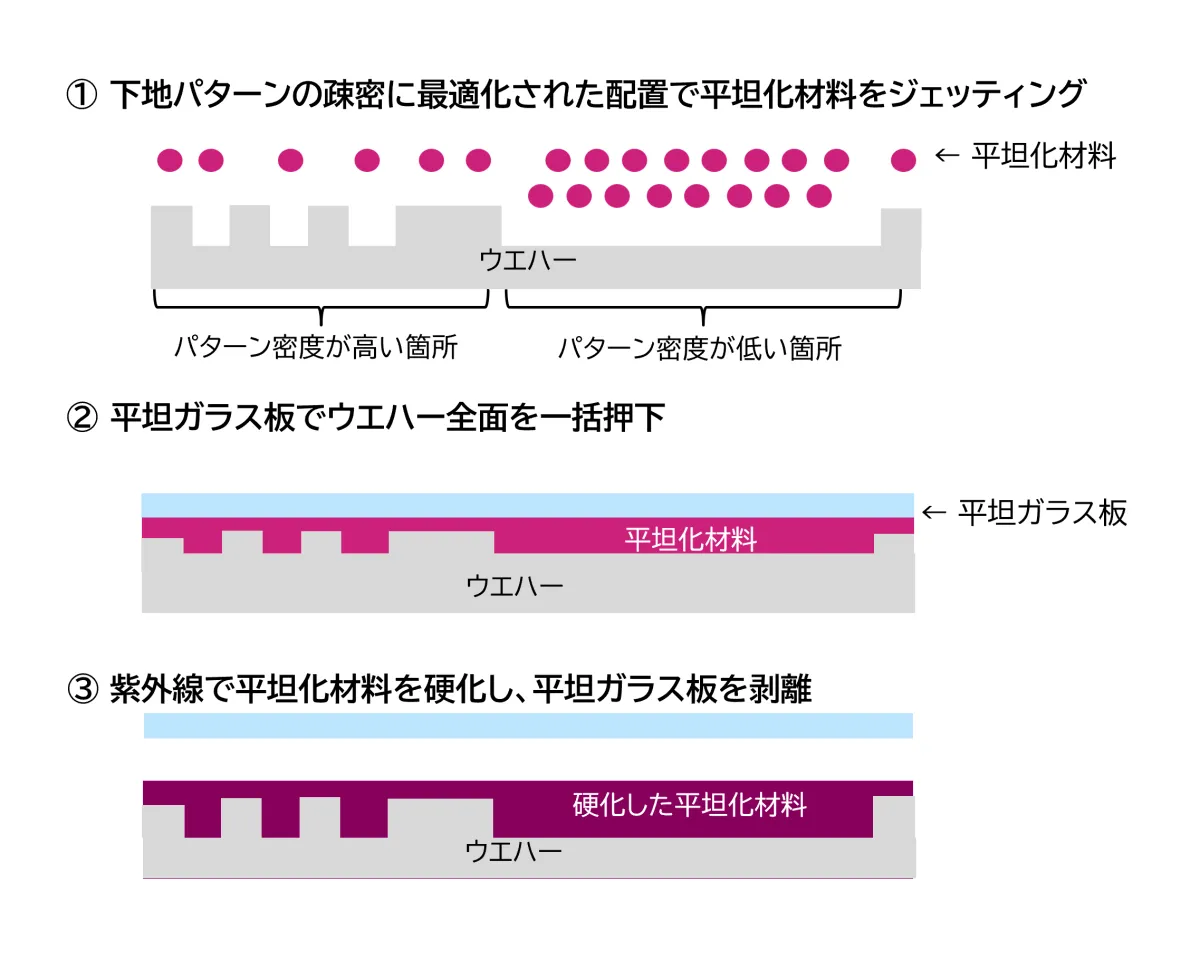
Leveraging its NIL technology, Canon has developed IAP, specifically designed for the planarization process. This technique involves applying a resist (polymer) layer to the wafer using an inkjet method. Subsequently, a mask with a circuit pattern is pressed against the wafer, similar to a stamping process, transferring the circuit design accurately.
What sets IAP apart is its capability to optimally position planarization materials (resin) according to the distribution of surface imperfections. By applying a planar glass plate over the inkjet-deposited resin, IAP achieves high-precision planarization across the entire surface of a 300mm wafer in a single stamping process. Remarkably, IAP can reduce surface roughness down to below 5nm, creating a much more uniform layer structure crucial for subsequent manufacturing steps.
Canon's developments hold great promise for the future of semiconductor manufacturing. The company intends to continue its research and development in semiconductor technologies and devices, aiming to contribute significantly to the evolution of semiconductors and the productivity of manufacturing environments.
Upcoming Presentation
For those interested in the latest advancements in this field, Canon, alongside its subsidiary Canon Nanotechnologies, is scheduled to present the IAP technology and its initial practical results at the SPIE Advanced Lithography and Patterning Conference, taking place on February 25, 2026, at the San Jose Convention Center.
This innovative technology not only represents a significant advancement for Canon but also sets the industry standard for future semiconductor processes, emphasizing the increasing need for precision in tech developments. With IAP, Canon is well-positioned to enhance the efficiency and effectiveness of semiconductor manufacturing on a global scale.
Topics Consumer Technology)
【About Using Articles】
You can freely use the title and article content by linking to the page where the article is posted.
※ Images cannot be used.
【About Links】
Links are free to use.