


Canon Showcases Innovations at SEMICON Japan 2025 with a Focus on Semiconductor Diversification
Canon's Participation at SEMICON Japan 2025
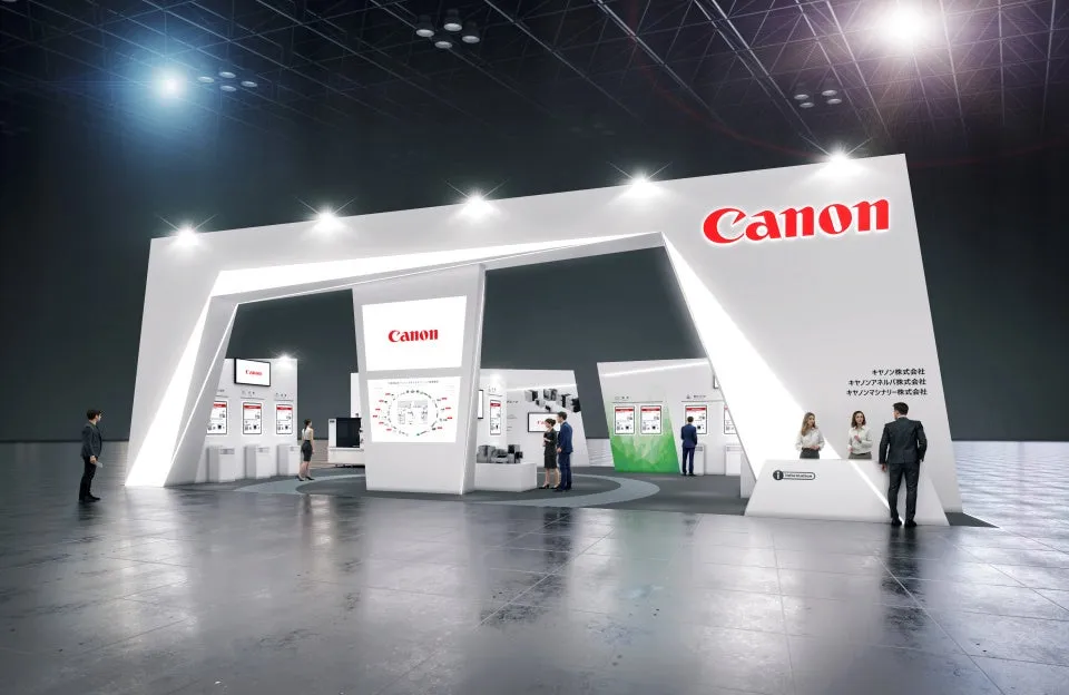
Canon, along with its subsidiaries Canon Anelva and Canon Machinery, will participate in the international semiconductor exhibition SEMICON Japan 2025, held at Tokyo Big Sight from December 17 to 19, 2025. This event has become a key platform for showcasing innovations in the semiconductor industry, as the demand for advanced manufacturing processes continues to evolve due to the expansion of applications such as generative AI.
Innovations in Semiconductor Manufacturing
As the semiconductor industry experiences growth, the need for refined manufacturing techniques has become increasingly vital. At Canon's booth, visitors will be introduced to a variety of advanced technologies that support next-generation semiconductor manufacturing. This includes equipment that enables miniaturization and energy-saving solutions utilizing nano-imprint technology, which allows for the formation of intricate circuit patterns in a cost-effective manner. Additionally, Canon will present advanced packaging solutions that cater to the high-density requirements of contemporary devices.
One of the highlights is the FPA-1200NZ2C, a semiconductor manufacturing device set to launch in October 2023. This device employs nano-imprint technology to form fine circuit patterns without incurring high production costs. Furthermore, attendees can explore the FPA-5520iV LF2 option, an exposure device tailored for advanced packaging and scheduled for release in January 2023. To provide an immersive experience, Canon will utilize its Mixed Reality (MR) system, known as MREAL, to showcase the internal exposure processes of their semiconductor exposure equipment.
Diverse Lineup from Canon's Industrial Group
Canon Anelva will exhibit the Adastra series, recognized with a Gold Award at the iF Design Award 2025 in the product category. This series is designed to cater to a wide range of film deposition processes and is set for release in October 2024. Attendees will also learn about the BC7300, an atomic diffusion bonding machine launched in June 2023, designed for wafer bonding. In addition, Canon Machinery will demonstrate its BESTEM-D610, a die bonder suitable for 12-inch wafers, which will be utilized in live demonstrations, showcasing the essential products within Canon’s diverse industrial lineup for semiconductor device manufacturing and packaging substrate production.
Commitment to Environmental Sustainability
Canon is dedicated to achieving net-zero CO₂ emissions across the entire product lifecycle by 2050. To support this goal, the company actively incorporates technologies that reduce environmental impact. Among these initiatives is the extended lifespan of equipment through part upgrades and virtualization technology, alongside UV-LED exposure options that contribute to decarbonization and the elimination of mercury. These eco-friendly efforts will be showcased prominently at the Canon booth, highlighting the company's commitment to sustainable semiconductor manufacturing practices.
SEMICON Japan 2025 Overview
- - Dates: December 17 (Wednesday) – 19 (Friday), 2025
- - Hours: 10:00 AM – 5:00 PM
- - Venue: Tokyo Big Sight
- - Admission Fee: Free (Pre-registration required)
Canon's booth will be located on the first floor of the South Exhibition Hall.

Topics Consumer Products & Retail)


【About Using Articles】
You can freely use the title and article content by linking to the page where the article is posted.
※ Images cannot be used.
【About Links】
Links are free to use.