



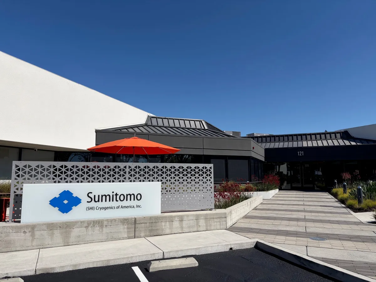
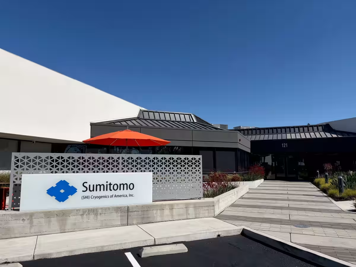
Opening of Semiconductor Subsystems and Components R&D Center in San Jose: A leap towards Innovation
Sumitomo Heavy Industries Expands R&D Efforts in Silicon Valley
In a strategic move to bolster its competitive edge in the semiconductor and robotics sectors, Sumitomo Heavy Industries has officially launched the Semiconductor Subsystems and Components R&D Center in San Jose, California. Scheduled to open in May 2026, this facility marks a significant step in the company’s continued commitment to innovation and collaboration.
Located within the premises of Sumitomo Cryogenics of America, Inc., the new R&D center aims to forge closer ties with American semiconductor equipment manufacturers and research institutions. By partnering with local innovators, Sumitomo Heavy Industries seeks to develop advanced technologies for next-generation semiconductor manufacturing equipment. The focus will be on enhancing the performance of components such as precision stages and motion components while addressing customer challenges in a timely manner.
Objectives of the New R&D Center
The establishment of the Semiconductor Subsystems and Components R&D Center is pivotal for Sumitomo Heavy Industries as it aims to:
- - Promote collaboration with U.S. partners engaged in semiconductor technology.
- - Accelerate technological advancements in semiconductor manufacturing processes.
- - Expand application areas of robotics and automation.
- - Create new business opportunities through strengthened partnerships.
These objectives underline the center's role as a nurturing ground for innovation that will ultimately benefit both Sumitomo Heavy Industries and its partners.
Advanced Facilities for Research and Development
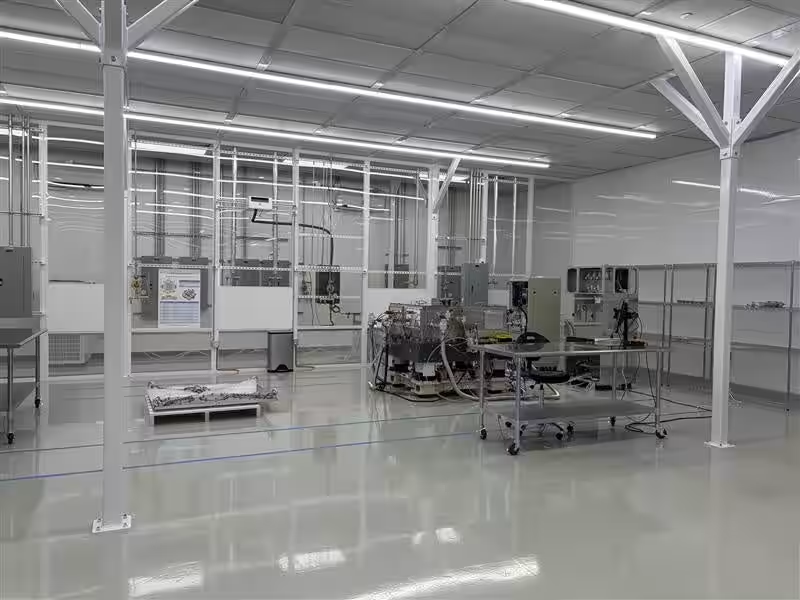
The new center features a state-of-the-art clean room environment with stringent requirements. Covering an area of 1,650 square feet (approximately 150 square meters), it achieves a cleanliness classification of Class 100 under the U.S. federal standard. This environment is crucial for conducting sensitive evaluations needed in precision stages and robotics technologies.
In addition to an ultra-clean atmosphere, the R&D center provides a low-vibration setting to ensure precise positioning and dynamic characteristics analysis of components at the nanometer level. Such advanced testing capabilities will enable collaborative product development and evaluation with U.S. partners, thereby ensuring that new solutions meet the high standards required in semiconductor manufacturing.
Overview of the Facility
- - Facility Name: Semiconductor Subsystems and Components R&D Center
- - Location: 121 Daggett Drive, San Jose, CA 95134, USA
- - Clean Room Specifications:
- Cleanliness Level: Class 100 (per Federal Standard 209E)
- Vibration Criterion (VC): VC-E, suitable for cutting-edge nanofabrication processes.
With its new R&D center, Sumitomo Heavy Industries is not only enhancing its research capabilities but also affirming its commitment to driving technological advancements in the semiconductor and automation industries. Through cooperative efforts and shared innovation, the company aspires to lead the way in a rapidly evolving market, ensuring a sustainable and technologically advanced future.
This initiative reflects an understanding of the critical role that collaboration plays in the success of the semiconductor industry, especially in a hub like Silicon Valley, where innovation and cutting-edge technology converge.

Topics Consumer Technology)
【About Using Articles】
You can freely use the title and article content by linking to the page where the article is posted.
※ Images cannot be used.
【About Links】
Links are free to use.