Explore the Latest Semiconductor Packaging Innovations and Technologies in Koyuki Hirakuta's New Book


Comprehensive Guide to Semiconductor Packaging and Assembly
Koyuki Hirakuta, a seasoned expert in semiconductor manufacturing, presents a detailed exploration of semiconductor packaging and assembly in his new publication, Comprehensive Guide to Semiconductor Packaging and Assembly: From Basics to Advanced Chiplet Technologies, published by CMC Research. This book serves as an essential resource for engineers, researchers, and students aiming to deepen their understanding of the semiconductor packaging industry.
Overview of the Book
Expected to release on September 10, 2025, this book is meticulously crafted in A4 format, comprising 112 pages and priced at ¥70,000 (tax included ¥77,000). For those seeking a more comprehensive experience, a bundled set containing the book and a CD is available for ¥120,000 (tax included ¥132,000). The ISBN for this enlightening read is 978-4-910581-68-2.
Highlights of the Book
The book covers:
- - Fundamental principles of semiconductor packaging to advanced applications.
- - Spotlight on innovative 2.5D/3D packaging and chiplet technologies.
- - Valuable practical insights gathered from years of hands-on experience in the field.
- - Analysis of actual failures, evaluation, and analytical methods used during the prototyping and development phases.
- - Discussion on environmental regulations, including RoHS and PFAS.
- - A forward-looking perspective on the future of semiconductor packaging.
The Importance of Semiconductors Today
Today, semiconductors are not merely components; they are crucial to our daily lives, powering everything from smartphones and AI devices to cars. As they evolve into key elements of economic security, the manufacturing processes require addressing increasing miniaturization challenges. Despite significant advancements to reach the 2nm threshold, the majority of semiconductors do not necessitate such technology. Instead, the integration of multiple chips using chiplet technology is driving the industry forward.
This book meticulously focuses on the ‘back end’ of semiconductor manufacturing — the packaging process, elucidating everything from foundational knowledge to advanced applications. Historically, semiconductor packages merely protected chips while facilitating external connections. However, driven by market demands, these packages have evolved, embracing multi-pin configurations, high functionality, and compact designs, transitioning from DIP to QFP and BGA formats. This evolution is meticulously chronicled in the book, along with an in-depth analysis of key manufacturing processes.
Insights from a Seasoned Expert
One of the significant attributes of this work is the wealth of experience and knowledge shared by the author, Koyuki Hirakuta. Anecdotes from his years working in semiconductor manufacturing provide a unique view of the challenges faced during development, accompanied by valuable lessons learned from failures. These firsthand experiences transform theoretical knowledge into applicable insights, particularly beneficial for engineers and researchers in the semiconductor industry.
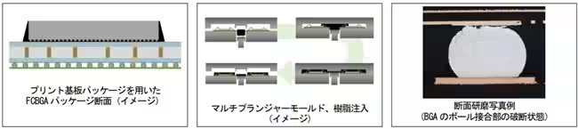
In addition, the book dives into common issues such as chip cracking, wire breaks, and popcorn cracks, detailing evaluation and analysis methods used during development. This information is vital for professionals aiming to enhance their expertise in semiconductor design and packaging.
Current Trends and Future Directions
Moreover, the text integrates robust discussions on contemporary trends, including initiatives to comply with environmental regulations such as RoHS and PFAS. The evolution of 2.5D/3D packaging and chiplet technologies is thoroughly examined, revealing strategic insights into their integration into future semiconductor packaging practices.
This publication aims to serve as a compass for aspiring semiconductor professionals, students looking to enter the industry, and those desiring a comprehensive understanding of semiconductor packaging — paving the path for enhanced knowledge and innovation in this rapidly evolving field.
About Koyuki Hirakuta
Koyuki Hirakuta is a highly regarded consultant and engineer in the semiconductor sector. With an extensive career spanning several reputable companies, including Fujitsu and Spansion Japan, Hirakuta has devoted his expertise to improving manufacturing quality and reliability in semiconductor packaging. His contributions extend to academia, where he engages with students and professionals, enriching their understanding of semiconductor technologies.
By combining theory with practical insights, Comprehensive Guide to Semiconductor Packaging and Assembly is poised to be an invaluable resource, connecting the dots between current practices and future innovations in the semiconductor domain.
Topics Consumer Technology)

【About Using Articles】
You can freely use the title and article content by linking to the page where the article is posted.
※ Images cannot be used.
【About Links】
Links are free to use.