


New Direct Quantification of Joint Strength in Semiconductor Devices by Toray Research Center
Toray Research Center's Innovative Analysis Service
The Toray Research Center (TRC), located in Nihonbashi, Tokyo, has launched a pioneering analytical service that provides direct quantification of joint strength within semiconductor devices' hybrid junctions. This groundbreaking method addresses a persistent challenge posed by the inner joint strength of real devices, which until now, has remained largely unquantifiable.
As the performance and integration demands for semiconductors increase, ensuring the reliability of the junction interface has become a critical challenge. The technology developed by TRC builds upon the nano-indentation method, previously systematized by Professor Inoue’s laboratory at Yokohama National University. To adapt this method for real devices, TRC has engineered a pre-processing technique that selectively exposes the junction interface through polishing and etching processes. This innovation opens up the possibility to directly evaluate the joint interface within complex layered structures, enabling significant contributions toward improving the reliability of hybrid junctions, understanding defect causes, and enhancing yield rates.
The Background of Semiconductor Reliability
In recent years, advancements in AI and high-performance computing have spurred a rapid evolution in semiconductor performance and density. The significance of 3D packaging technology, which connects stacked chips, has gained substantial importance, with hybrid junctions at the core. Hybrid junctions facilitate simultaneous electrical connections between metal wiring (predominantly copper) and adjacent insulating layers (such as SiO₂), allowing for dense and low-resistance connections essential for high-performance 3D implementations. However, assessing the joint strength at the junction interface has been challenging due to its minute dimensions, typically ranging from nano to micrometers, and the fact that these interfaces often lie buried inside the device, making them difficult to evaluate under real-device conditions.
Prior joint strength evaluation methods, such as the Double Cantilever Beam (DCB) method, have limitations as they test simplified model samples or only the edges of wafers. This restriction hampers the ability to obtain reliable assessments reflective of actual multi-layered structures and device configurations, illustrating the need for a feasible evaluation technology applicable to real devices.
TRC's Technological Advancements and Analysis Examples
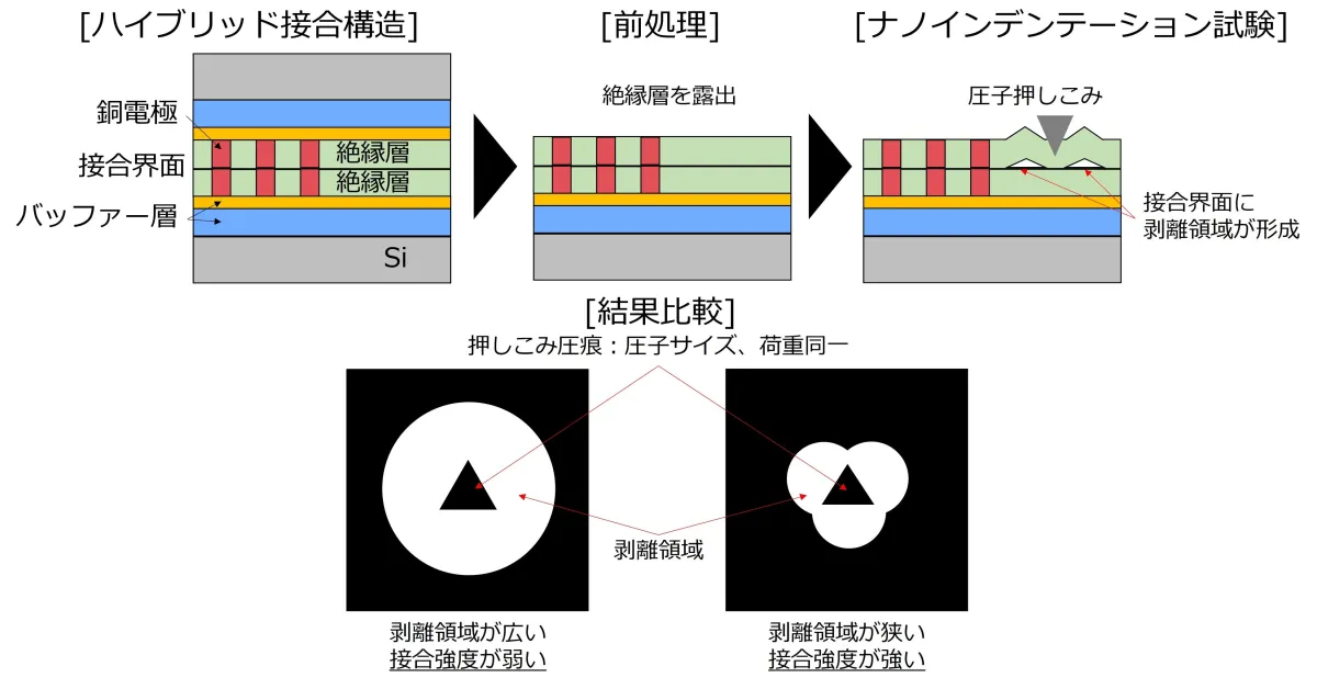
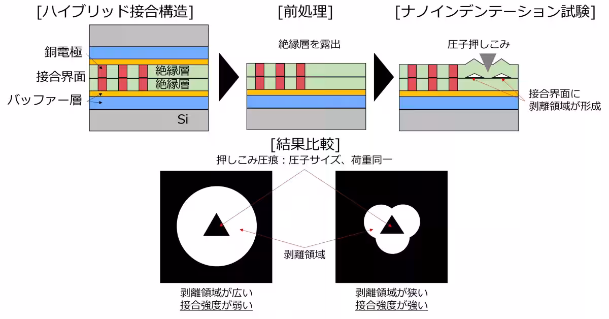
In response to these challenges, TRC harnesses insights from the nano-indentation method to develop a unique evaluation technique tailored for real devices. The approach involves systematically exposing the target junction interface according to the sample's layered structure and material characteristics by employing a combination of polishing and etching processes.
With exposed junction interfaces, a nano-indentation test can be conducted. During this test, as the indenter penetrates, delamination occurs at the interface. By observing and quantifying the shape and size of the delaminated region, the joint strength can be accurately assessed. A lower joint strength results in an expanded delamination area, whereas a higher strength restricts delamination, leading to a smaller region of fracture. Such correlations allow for an intuitive understanding of the variations in strength within actual device structures.
This innovative combination of pre-processing techniques with nano-indentation evaluation not only enables the quantitative assessment of joint strength in real device architectures but also captures the subtleties of interface reliability with precision, which were previously challenging to determine.
Future Prospects for the Service
This novel evaluation service offers incredible potential, including:
- - Quantifying variability in joint strength
- - Identifying locations and mechanisms of joint failures
- - Providing direct feedback for optimizing joining conditions
Through this technology, TRC aims to advance the development of cutting-edge packaging technologies in semiconductor and material manufacturing sectors, further promoting the sophistication of interface evaluation technologies.
Explanation of Terms
1. Hybrid Junction: A semiconductor connection technology that combines electrical connections between metal wiring (mainly copper electrodes) and joins insulating layers simultaneously, thereby enabling high density and reduced resistance, contributing to enhanced performance in 3D implementations.
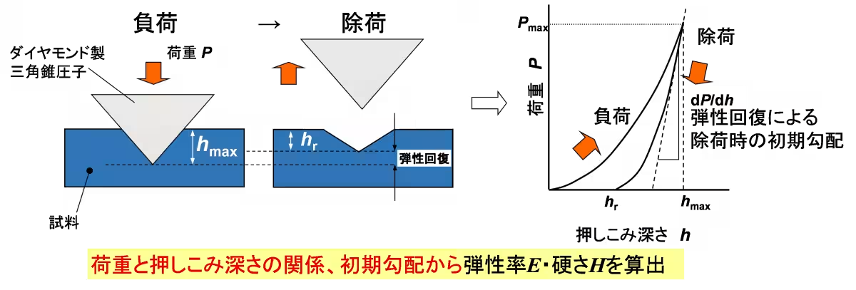
2. Nano-Indentation Method: A technique where a diamond tip is pressed into the material's surface to derive metrics like elasticity (Young's modulus) and hardness from the relationship between load and displacement. Widely utilized for evaluating mechanical properties in thin films or micro-regions.
3. Double Cantilever Beam Method (DCB): An evaluation method involving the opening and peeling of samples shaped like wedges to assess joint strength based on the peeling behavior. Commonly applied to simple layered structures or model specimens.
Topics Consumer Technology)


【About Using Articles】
You can freely use the title and article content by linking to the page where the article is posted.
※ Images cannot be used.
【About Links】
Links are free to use.