


Japan Develops Advanced Pilot Line for Cutting-Edge Transistor Prototyping
Japan Introduces Cutting-Edge Transistor Pilot Line
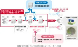
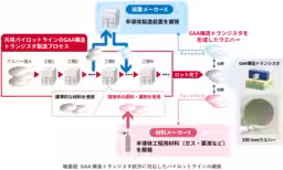
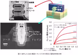
In an exciting development, the National Institute of Advanced Industrial Science and Technology (AIST) has successfully created Japan's first shared pilot line for advanced semiconductor prototyping. This pilot line, supported by funding from the New Energy and Industrial Technology Development Organization (NEDO), allows various stakeholders, including companies and universities, to conduct technology verification on cutting-edge transistors utilizing the gate-all-around (GAA) structure.
The new shared pilot line, built specifically for 300 mm silicon wafers, presents a unique opportunity for semiconductor device and material manufacturers to prototype and test novel devices. The primary objective is to enhance Japan's capabilities in developing top-tier logic semiconductors, responding to the growing demands for enhanced performance in this sector due to advancements in AI technology.
Unique Features of the Pilot Line
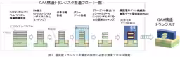
The defining characteristic of this pilot line is its ability to facilitate the prototyping of GAA structure transistors, which are deemed critical for future semiconductor technologies. This initiative marks a significant advance in Japan's semiconductor manufacturing landscape, as it enables local manufacturers to apply their proprietary processes and materials in a unified manufacturing setting.
Furthermore, this shared resource aims to bolster research and development efforts among Japanese semiconductor firms and academic institutions, thereby strengthening their international competitiveness, particularly for manufacturers that account for a substantial share of the global market.
Evolution of Semiconductor Manufacturing
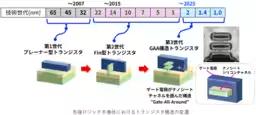
The transition from planar FinFET structures to multi-layer ultra-thin silicon channels capped by a GAA structure reflects the current trend among major global semiconductor manufacturers. This shift is crucial for achieving better performance while reducing power consumption, leaving Japan's semiconductor manufacturers at the forefront of this technological transition. However, challenges persist, especially given the complexities of prototyping these advanced structures, which often require significant capital investment and advanced fabrication techniques.
Collaboration for Innovation
The establishment of this pilot line has been a collaborative effort involving three leading domestic semiconductor manufacturing equipment manufacturers: Tokyo Electron, SCREEN Semiconductor Solutions, and Canon. Their collaboration is not only an impressive initiative to enhance each company's technological capabilities but also serves as a platform through which numerous companies can pool resources for R&D.
By providing access to this shared pilot line, AIST aims to create an ecosystem conducive to innovation where companies can independently validate and refine their electronic design processes and associated materials. This is particularly important in a sector where reliance on cross-border partnerships with overseas laboratories has often forced companies to expose sensitive intellectual property and proprietary technologies.
Future Directions
Looking ahead, the AIST intends to further enhance the functionalities of the pilot line by refining the dimensions of gate electrodes and successfully integrating both n-channel and p-channel transistors as part of a complementary metal-oxide-semiconductor (CMOS) architecture. Reinforcing the collaboration between industry and academia within this framework will also serve as a breeding ground for nurturing the next generation of engineers and researchers in the semiconductor field.
In summary, this pilot line represents a critical step forward for Japan's semiconductor industry. It not only enables rigorous testing and prototyping of next-generation transistors but also entrenches Japan's position as a key player in the global semiconductor supply chain. The outcomes of this initiative are expected to be shared at the AIST Symposium in November 2025, marking a milestone in Japan's semiconductor innovation landscape.
For more information about this project, please visit the AIST press release.
Topics Consumer Technology)


【About Using Articles】
You can freely use the title and article content by linking to the page where the article is posted.
※ Images cannot be used.
【About Links】
Links are free to use.