Upcoming Seminar on Semiconductor Packaging Technology: Trends and Innovations


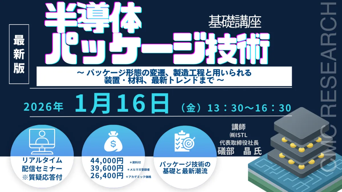
Upcoming Seminar: Fundamental Course on Semiconductor Packaging Technology
Date and Time: January 16, 2026 (Friday) from 13:30 to 16:30
Format: Live Zoom Webinar (with materials included)
Do not miss out on the enlightening seminar brought to you by CMC Research! This session is tailored for engineers, marketers, and anyone eager to understand the fundamentals of semiconductor packaging technology from the ground up. Leading the seminar will be Akira Isobe, CEO of ISTL, who will guide participants through the intricate world of semiconductor packaging.
Seminar Overview
The seminar, titled "Fundamental Course on Semiconductor Packaging Technology: Evolution of Package Types, Manufacturing Processes, and Latest Trends," covers several critical aspects:
- - Historical evolution of semiconductor packaging technologies
- - Manufacturing processes and the essential materials and equipment involved
- - Cutting-edge packaging technologies including chiplets and optoelectronic integration
Completing this seminar will provide you with a comprehensive grasp of both the current state and future directions of the industry, crucial for anyone looking to thrive in semiconductor technology.
What You Will Learn
1. The evolution of semiconductor packaging technologies and their historical context.
2. An overview of semiconductor packaging manufacturing processes, materials, and technologies.
3. Insights into next-generation packaging technologies and anticipated trends.
Target Audience
This seminar is particularly beneficial for:
- - Engineers keen on mastering semiconductor packaging techniques.
- - Sales and marketing professionals seeking to enhance their understanding of the industry.
Investment
- - General Admission: ¥44,000 (tax included)
- - Newsletter Subscribers: ¥39,600 (tax included)
- - Academic Rate: ¥26,400 (tax included)
Seminar Schedule
The program includes the following topics, interspersed with breaks:
1. Role of Semiconductor Packages
- Pre and post-process roles in packaging
- Evolution of substrate mounting methods
- Requirements for semiconductor packaging
2. Evolution and Element Technologies of Semiconductor Packages
- The transformation in packaging as mobile devices and PC technology advanced
- STRJ package roadmap
- Descriptions of various package types: DIP, QFP, TCP, BGA, WLCSP, etc.
- Key element technologies for packaging manufacturing: back grinding, dicing, die bonding, wire bonding, molding, bump technology, etc.
3. Latest Packaging Technologies
- Necessity for advanced packaging technologies due to limitations in Moore's Law
- Various System-in-Package (SiP)
- Insights on Fan-Out Wafer Level Packages (FOWLP) and Chip-on-Wafer-on-Silicon (CoWoS)
- Understanding chiplets and Embedded Multi-die Interconnect Bridge (EMIB)
- The integration of optoelectronic packaging
- The future direction of packaging technologies
Instructor Background
Akira Isobe is an esteemed figure in semiconductor processing technology, having decades of experience in the industry:
- - Joined NEC in 1984, working on semiconductor process and multi-layer wiring technologies.
- - Previous positions at Tokyo Seimitsu and Nitta Hass, leading technical innovation teams.
- - Founded ISTL in 2015, currently serving as CEO.
Join us on January 16 for this essential seminar that promises to enhance your understanding of semiconductor packaging technology. Gain insights that are critical for anyone involved in research and operations within this rapidly advancing field.
Registration Details
To register for the seminar, visit CMC Research's website where you can find more information and obtain the viewing URL post-registration.
For queries, a Q&A session will be included in the seminar, ensuring that all your questions are addressed.
For more updates on upcoming webinars and seminars, be sure to check our website frequently!
Topics Other)

【About Using Articles】
You can freely use the title and article content by linking to the page where the article is posted.
※ Images cannot be used.
【About Links】
Links are free to use.