Exploring Advanced Crystal Defect Evaluation Techniques for Next-Gen Power Semiconductors


Exploring Advanced Crystal Defect Evaluation Techniques
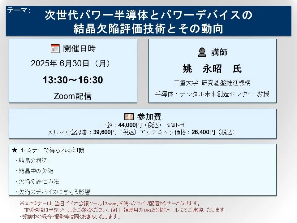
On June 30th, 2025, the renowned CMC Research will host a live webinar titled 'Next-Generation Power Semiconductor and Power Device Crystal Defect Evaluation Techniques and Trends.' This important event, commencing at 1:30 PM (JST), will welcome Professor Yao Yozhou from Mie University, a leading expert in the field. The session will be conducted via Zoom and is aimed at researchers and engineers engaged in the evaluation of semiconductor crystal defects.
Seminar Details
Registration Fees:
- - General Admission: ¥44,000 (tax included)
- - CMC Newsletter Subscribers: ¥39,600 (tax included)
- - Academic Price: ¥26,400 (tax included)
This interactive seminar promises to enrich your knowledge of crystal structure, evaluate crystal defects, and detail methods to assess their impact on device performance. Additionally, a Q&A session will be available for participants to seek clarifications on intricate topics.
Knowledge Gained from the Seminar
During the seminar, attendees will learn about:
- - The structure of crystals
- - Types of defects present in crystals
- - Evaluation methods for defects
- - The negative impacts of defects on devices
Target Audience
This seminar is ideal for researchers and engineers focusing on evaluating crystal defects in semiconductors and power devices. Coordinator and attendees are encouraged to engage actively in discussions to leverage collective expertise.
Focus of the Presentation
Professor Yao Yozhou's presentation will highlight wide-bandgap semiconductors such as 4H-SiC, GaN, β-GaO, and AlN. These materials demonstrate remarkable performance characteristics, including high power density, low loss, and high-temperature stability. There has been significant advanced research into these power devices, yet challenges still exist in crystal growth due to strong covalent bonding, often resulting in a high density of crystal defects post-growth.
Some lattice defects can adversely affect device performance and reliability, underscoring the critical importance of accurately identifying defect distributions and types. The seminar will address identifying killer defects that significantly impair device characteristics which can then be fed back into crystal growth and device fabrication processes.
Professor Yao will explain evaluation techniques, addressing their principles, applications, and challenges. Furthermore, he will present case studies showcasing the latest evaluation examples, such as radiographic X-ray topography, etch pit methods, Transmission Electron Microscopy (TEM), and multiphoton excitation microscopy.
How to Register
Interested participants can register for the seminar on CMC Research’s website, from where a viewing URL will be forwarded via email after registration. For more details, please visit our URL provided in the announcement.
Seminar Program Overview
1. Introduction
1.1 Wide-Bandgap Semiconductors for Power Devices
1.2 Crystal Defects in Semiconductors
1.3 Evaluation Methods and Application Areas
2. Evaluation Techniques
2.1 Selective Chemical Etching (Etch Pit Method)
2.2 Transmission Electron Microscopy
2.3 Multiphoton Excitation Microscopy
2.4 X-ray Diffraction and X-ray Topography
2.5 Other Evaluation Methods
3. Device Evaluation
3.1 Defects in Devices
3.2 Evaluation Methods for Defects in Devices
3.3 Negative impacts of Defects on Devices
4. Summary
About the Speaker
Professor Yao Yozhou has a notable academic background, having completed his doctorate at the University of Tsukuba in 2007 and serving as a postdoc at the National Institute for Materials Science. He has dedicated his career to developing evaluation methods for the next generation of power device wide-gap compound semiconductors and is a permanent member of several scientific committees, ensuring that his teachings are at the forefront of technology development in this field.
For updates on upcoming seminars and additional resources, follow CMC Research to help articulate the journey of science and technology. Join us in embracing innovation and transformation in semiconductor technology!
Topics Consumer Technology)
【About Using Articles】
You can freely use the title and article content by linking to the page where the article is posted.
※ Images cannot be used.
【About Links】
Links are free to use.