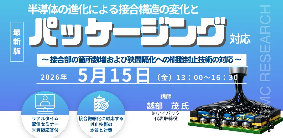
Upcoming Seminar on Semiconductor Evolution and Packaging Technology: Key Insights and Innovations


Upcoming Seminar: Changes in Semiconductor Packaging
On May 15, 2026, a valuable live seminar will be hosted by CMC Research, focusing on the evolution of semiconductors and the corresponding advancements in junction structures and packaging techniques. The event will be conducted via Zoom from 13:00 to 16:30, providing an in-depth look into how packaging technologies have evolved to accommodate the increasing complexity in semiconductor design.
Seminar Details
- - Date and Time: May 15, 2026 (Friday) from 13:00 to 16:30
- - Platform: Zoom (materials provided)
- - Lecturer: Shigeru Koshibe, President of iPack Co., Ltd.
- - Theme: "Changes in Junction Structures and Packaging Technologies due to Semiconductor Evolution: Responses to Increased Junction Count and Narrow Spacing Using Resin Sealing Technologies"
This seminar aims to clarify the core designs of junctions and sealing technologies crucial for WLP (Wafer Level Package) and 3D packaging eras. It will cover various poor assembly mechanisms associated with high integration, offering insights directly relevant to development, evaluation, and manufacturing challenges in the semiconductor industry.
Registration Fees
- - General Admission: ¥44,000 (tax included)
- - Newsletter Subscribers: ¥39,600 (tax included)
- - Academic Rate: ¥26,400 (tax included)
Participants will also have the chance to engage in a Q&A session, making this seminar an excellent opportunity for professionals in research and business to enhance their knowledge on semiconductor technology.
Acquired Knowledge
Participants will gain insights on:
- - The development history and trends of semiconductor packaging.
- - Changes in semiconductor junction structures and corresponding packaging technology adaptations.
- - The evolution of semiconductor packaging and the development and challenges of resin sealing technologies.
Target Audience
This seminar is relevant for individuals involved in any aspect of semiconductor technology, whether in sales, engineering, or manufacturing. It is also ideal for anyone eager to understand advancements in semiconductor packaging technology or the Bumping Technology critical for semiconductor integration.
Seminar Agenda
The seminar will be divided into informative segments, with breaks in between:
1. Evolution of Semiconductor Packaging and Junctions
- Development background focusing on high integration and density.
- Various types of packages including WLP, PLP, and composite packaging.
- Connections between packages and circuit boards and how advances in reliability are verified.
2. Adaptation of Semiconductor Packaging Technology
- An overview of sealing technologies and materials, detailing the development history and their application.
- Evaluation of sealing materials, including response to challenges like wide-area application and minimal gap injection.
- Identification of defective conditions in composite package assembly and their corresponding analysis.
About the Lecturer
Shigeru Koshibe graduated from Osaka University in 1974 and embarked on a remarkable career in semiconductor sealing materials. He has over 200 filings for industrial property and has written around 60 books in this field, firmly establishing himself as an authority on semiconductor packaging technologies. His experience in consulting and developing materials for both semiconductor and optical fields will offer attendees invaluable insight.
How to Register
Please visit CMC Research’s dedicated seminar page to register. After registration, participants will receive a URL for viewing the live stream via email.
This seminar promises to enhance understanding and foster discussion around semiconductor packaging challenges and solutions in our ever-evolving tech landscape. Join us to stay ahead in this critical field.
Topics Consumer Technology)
【About Using Articles】
You can freely use the title and article content by linking to the page where the article is posted.
※ Images cannot be used.
【About Links】
Links are free to use.