



JASP Introduces Wireless Temperature Sensor Wafer for Semiconductor Manufacturing in Japan
JASP Unveils Revolutionary Wireless Temperature Sensor in Japan
In a significant move for the semiconductor manufacturing sector, JASP has launched a wireless temperature sensor wafer developed by the South Korean deep-tech company MNTek. This innovative product will cater to the increasing demands of semiconductor devices in today’s digital landscape, where high-performance and compact designs are paramount due to the rise of technologies such as AI, data centers, autonomous driving, and 5G/6G communications.
Addressing Semiconductor Manufacturing Challenges
As semiconductor production processes evolve, there is a growing need for precise nano-level processing. One critical area that requires meticulous control is the temperature management during the Plasma etching phase. Ensuring the right temperature within the etching chamber is essential, as slight variations can impact etching uniformity and dimensional accuracy, leading to quality discrepancies across different equipment and conditions.
The newly introduced wireless temperature sensor wafer aims to tackle these challenges faced by semiconductor and manufacturing equipment companies. Its unique design enables it to measure temperature distributions accurately and in real-time, even in complex high-frequency (RF) plasma environments that are not easily navigable with traditional methods.
Cutting-edge Design Features
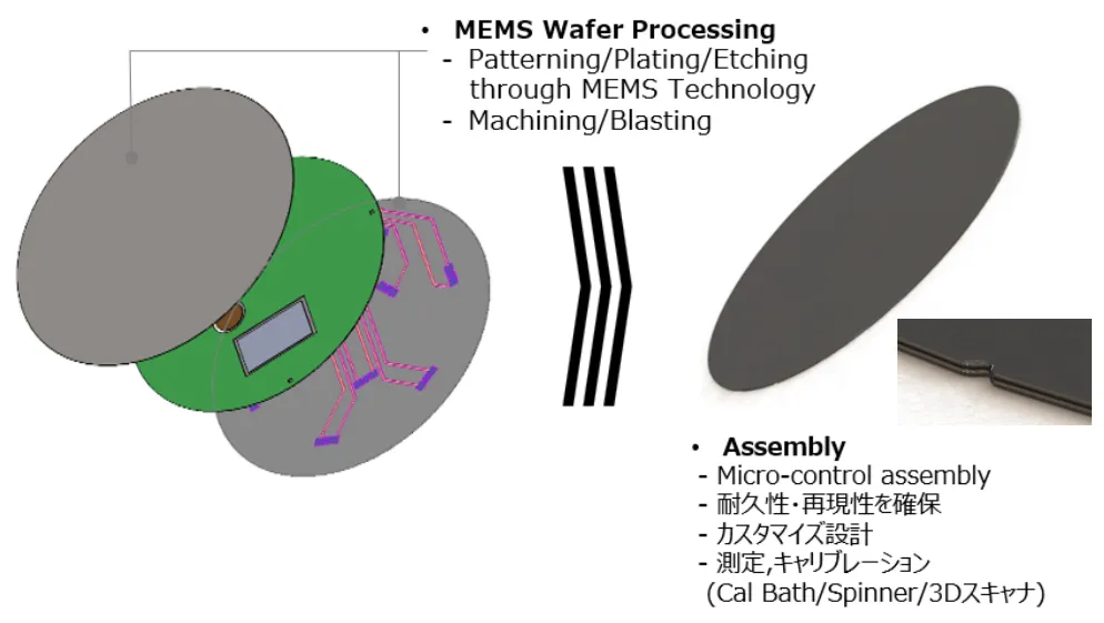
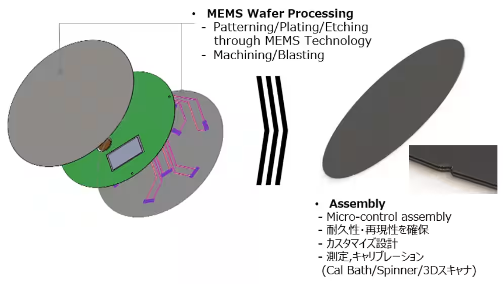
The wireless temperature sensor wafer is designed to match the size and shape of standard 300mm silicon wafers. It incorporates temperature sensors, electronic circuits, and batteries within a dummy wafer, all encased in a silicon cover that allows for a remarkably thin profile of under 1.4mm. This design enables it to be handled like traditional production wafers using robotic transport, thus allowing for seamless integration into existing manufacturing workflows.
Post-measurement, temperature data can be wirelessly transmitted via specialized software, significantly boosting operational efficiency compared to conventional wired methods.
High-Precision Sensing Technology
Equipped with MNTek's proprietary technology, the wireless sensor wafer utilizes advanced MEMS technology and precision assembly techniques. Each wafer can hold up to 65 temperature sensors, providing detailed heat mapping across its surface. Furthermore, it features RF shielding that ensures reliable measurements in environments with up to 7kW of dual-source RF plasma.
Clients can also customize sensor count, measurement ranges, RF resistance, and product lifespan to suit their specific needs, showcasing the wafer's flexible design.
Contribution to Process Optimization
The real-time temperature data gathered by these sensor wafers is invaluable for a range of applications, including temperature gradient analysis between etching chambers, performance evaluation of electrostatic chucks, and verifying setups post-preventive maintenance. By enabling quantitative insights into the operational state of machinery, these sensors play a crucial role in optimizing process conditions, stabilizing product quality, enhancing equipment uptime, and ultimately improving yield in semiconductor manufacturing.
Additionally, when combined with dedicated analysis software, they assist with rapid root cause analysis and equipment diagnostics on the production floor, driving productivity gains.
Differentiating Features from Competitors
What sets MNTek's product apart from standard temperature measurement devices is its tailored approach to meet individual client specifications. From sensor capabilities to RF parameters, wafer lifespan, and memory capacity, the options for customization are plentiful. Each device also comes standard with wireless data communication capabilities, along with comprehensive support for troubleshooting, calibration, and product replacement, all grounded in a
Topics Other)
【About Using Articles】
You can freely use the title and article content by linking to the page where the article is posted.
※ Images cannot be used.
【About Links】
Links are free to use.