




JFE Tech Research Launches Innovative Non-Destructive Analysis Using 3D X-Ray Microscopy
JFE Tech Research Unveils Advanced 3D X-Ray Microscopy
Significant Leap in Non-Destructive Analysis
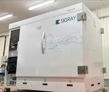
JFE Tech Research, headquartered in Chiyoda, Tokyo, officially launched its non-destructive analysis services utilizing the revolutionary 3D X-ray microscope, the ApexHybrid-210TM from Sigray, USA. Starting from August 2026, this innovative tool is designed to address the growing demand for detailed internal structure observation in fields like solid-state batteries and semiconductor packaging.
Background and Emerging Needs
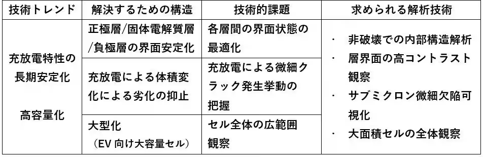
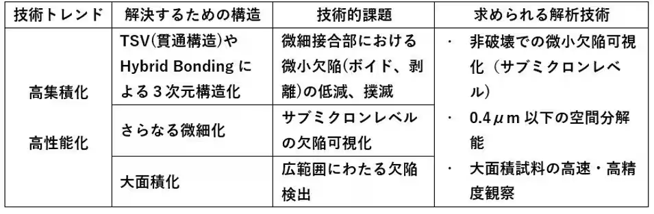
The recent surge in demand for compact, high-capacity electronic devices has prompted advancements in 3D structuring and multilayering of materials and devices. Consequently, there’s a pressing need for high-resolution non-destructive analysis technologies that allow the observation of intricate internal structures without the need for sample destruction. Traditional methods faced critical issues:
- - Time-consuming sample cutting and preparation.
- - Limited local observations that lack a comprehensive view.
- - Lengthy development cycles due to the repeated processes of prototyping, performance evaluation, destruction, and analysis.
This context has amplified the requirement for non-destructive 3D analysis technologies that can visualize sub-micron-level defects swiftly without sample cutting.
Innovations of the New System
The ApexHybrid-210TM is a hybrid model that integrates orthogonal CT and angled CT (laminography) imaging modes in a single device. Featuring Sigray's unique precision angle-controlled laminography, this microscope offers high-contrast and high-resolution images even when observing large-area samples, eliminating the need for cutting.
Key Features of the ApexHybrid-210TM
1. Large Area Sample Capability: The device can observe large samples with a maximum diameter of 300mm and thickness of 20mm without cutting, providing high-quality non-destructive observation thanks to precision angle-controlled laminography.
2. Industry-Leading Resolution: Equipped with a state-of-the-art nano-focus X-ray source and a proprietary high-sensitivity detector, this system achieves an unprecedented spatial resolution of 0.40μm, clearly visualizing fine structures and defects in samples, particularly in battery applications requiring high-aspect ratio evaluations.
3. Significantly Increased Efficiency: By combining orthogonal CT and angled CT techniques, the system enhances internal structure observations by 10 to 100 times when compared to traditional methods like SEM, effectively shortening research and quality assurance processes.
Case Analyses
Battery Sector
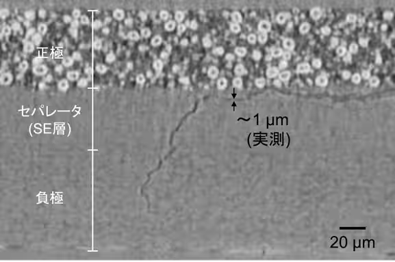
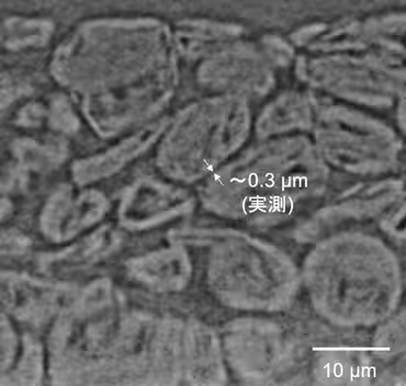
In solid-state batteries, the research revealed internal cracks appearing during charge-discharge cycles. Using orthogonal CT, cracks from the positive electrode layer towards the negative electrode layer were visualized non-destructively, detecting fine cracks measured under 2μm in size. This capability was further validated through traditional measurements of lithium-ion battery anodes, achieving visualization of structures under 0.4μm.
Electronic Devices Sector
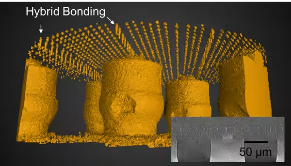
The system successfully visualized non-destructively hybrid bonding structures within commercially available CPU substrates using angled CT mode. The wiring structures, with widths below 2μm, were clearly captured, demonstrating the system's ability to meet emerging needs in evaluating wiring connections at the micro-level amidst advancing stacking technologies.
Potential Applications and Expected Impact
The advanced non-destructive analysis provided by the ApexHybrid-210TM is anticipated to benefit a diverse range of industries, particularly in fields necessitating rapid, high-precision inspections without sample damage. Expectation areas include:
- - Research and Development: Optimizing internal structures and accelerating evaluation cycles.
- - Quality Assurance: Conducting full or sampling inspections non-destructively and analyzing variance causes in products.
- - Failure Analysis: Identifying cracks, peeling, and bonding failures, facilitating root cause analysis before destructive testing.
Target Areas
- - Non-destructive inspections of semiconductor materials and related components like wafers.
- - Analysis of various battery cells and components including solid-state batteries, lithium-ion batteries, and fuel cells.
- - Fine structural evaluations of metals, composites, and biomaterials.
Future Developments
JFE Tech Research aims to further develop this solution into a comprehensive offering that incorporates enhanced analytical data (including quantitative and AI analyses) and collaborates with other evaluation methods, ultimately optimizing the entire R&D and product development processes for manufacturers.
For more information about the analysis services, visit JFE Tech Research's website.
Furthermore, detailed information about the devices can be found on Canon Marketing Japan’s official product page: ApexHybrid-200.
About JFE Tech Research
- - Company Name: JFE Tech Research Co., Ltd.
- - Headquarters: 1-6-1 Otemachi, Chiyoda, Tokyo, Japan, 4th Floor Otemachi Building
- - CEO: Kazuhiko Hanazawa
- - Business Focus: From experimental plans to measurement, data analysis, evaluation, and consulting, specializing in measurement device development.
- - Website: JFE Tech Research
- - Note: JFE Tech On Note
Contact Information
For inquiries about this matter, please reach out to the Sales Division of JFE Tech Research: Contact Us | Email: [email protected]

Topics Consumer Technology)
【About Using Articles】
You can freely use the title and article content by linking to the page where the article is posted.
※ Images cannot be used.
【About Links】
Links are free to use.