Strengthening Semiconductor Workforce Through Japan-India Collaboration in Kyushu and Tohoku


Strengthening Semiconductor Workforce Through Japan-India Collaboration
In early July, a delegation of seven officials and university professors from India's government focused on the semiconductor industry visited the Kyushu and Tohoku regions of Japan. Organized by the Japan International Cooperation Agency (JICA), this visit was designed to evaluate the current state of semiconductor manufacturing and workforce development initiatives in Japan, with the ultimate goal of addressing the ongoing shortage of skilled labor in both India and Japan.
This visit aligns with a broader vision of 'Connecting the World Through Trust' as Japan seeks to enhance international cooperation through its development aid initiatives. With the Indian semiconductor market rapidly expanding, driven by increasing demands in AI, smartphones, and automobile components, Japan aims to ramp up collaboration with India to overcome mutual challenges, particularly in workforce shortages.
Background of the Project and Future Outlook
As reported, both the Indian market and the international semiconductor ecosystem have been shifting, especially in light of geopolitical tensions. Recent figures indicated that India's shipments of iPhones to the U.S. surpassed those from China, highlighting a significant pivot towards Indian production capabilities in the semiconductor and smartphone sectors. Indian Prime Minister Modi is pushing for the India Semiconductor Mission (ISM), which includes substantial government backing to foster domestic semiconductor manufacturing.
In response to this escalating demand, JICA is set to begin a Japan-India Semiconductor Supply Chain Information Gathering Survey in May 2024. This prepares the groundwork for durable cooperative frameworks in workforce training initiatives between academic, government, and industry sectors in both countries.
Visit Highlights and Engagements
During the visit, multiple key organizations were highlighted:
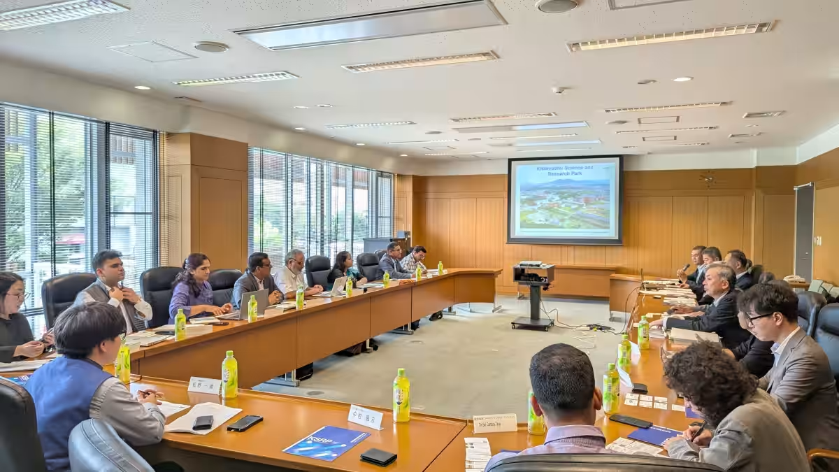
FAIS (Kyushu Industrial-Academic Promotion Organization) - July 8
FAIS in Kitakyushu introduced its G-CITY Strategy, focusing on fostering semiconductor talent through extensive collaboration with universities and industries. With its state-of-the-art cleanroom facilities, FAIS offers innovative training programs, capturing attention from the Indian delegates. Dr. Manish Kumar Huda, representing India's Ministry of Electronics and Information Technology, expressed interest in leveraging Kitakyushu's excellent resources for cutting-edge training programs.
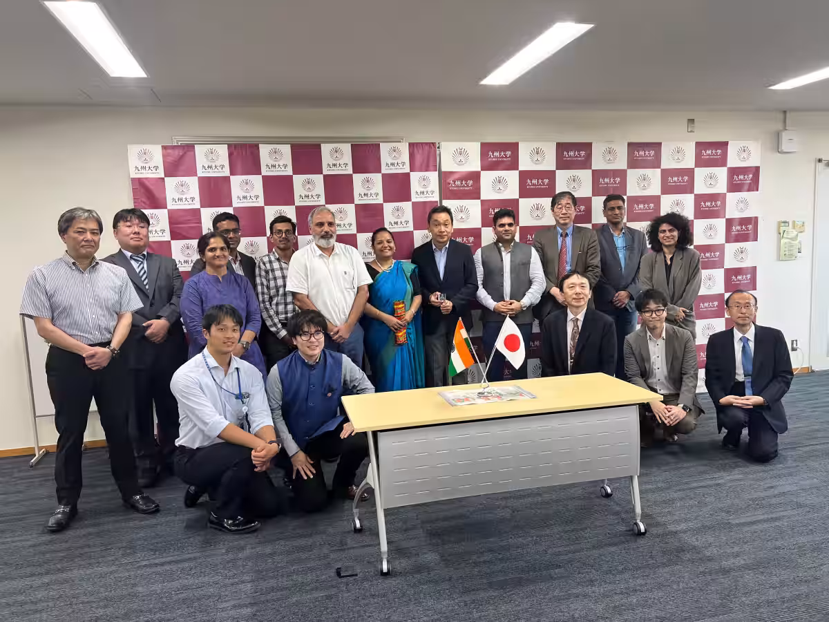
Kyushu University
At Kyushu University, discussions led by six professors centered on semiconductor research, elucidating potential academic exchanges and cooperation between Indian institutions, such as the Indian Institute of Technology Gandhinagar. Professor Haruki Kanaya from Kyushu University suggested exploring study abroad programs to deepen connections established during this collaboration.
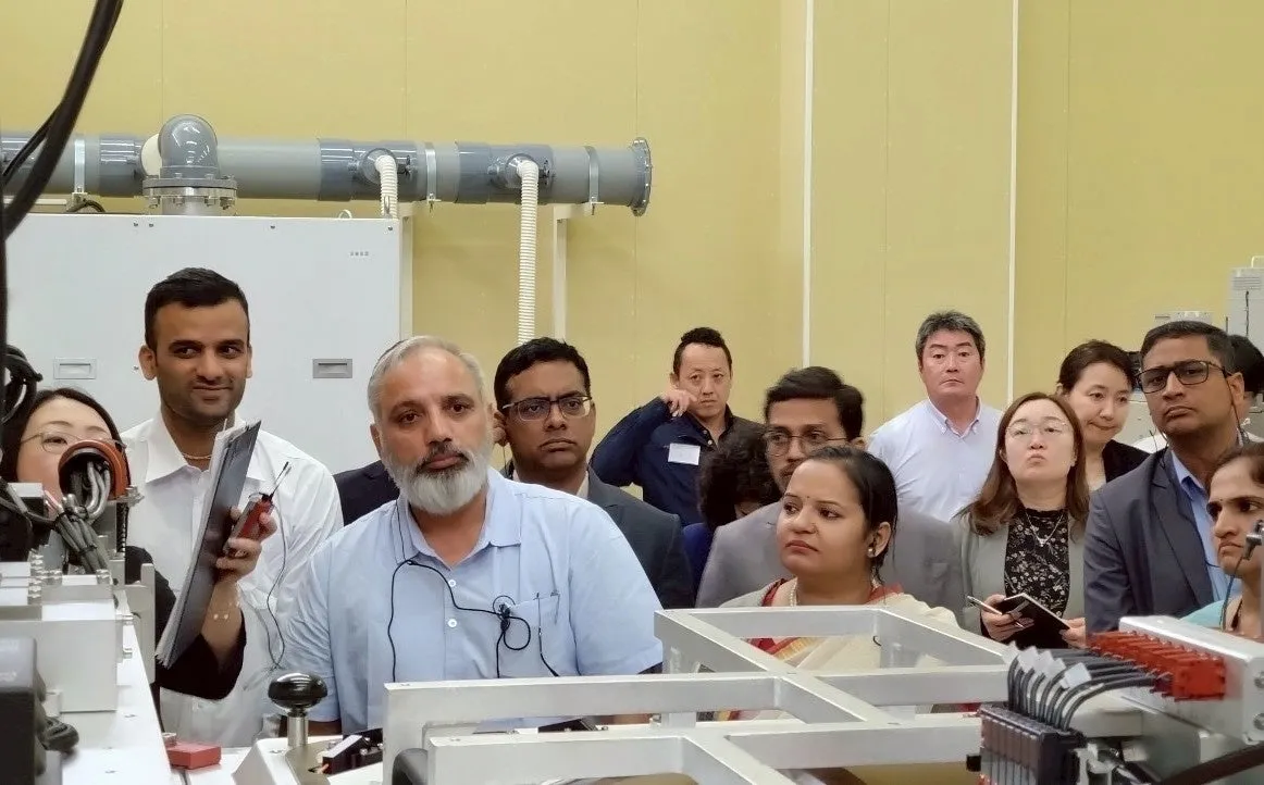
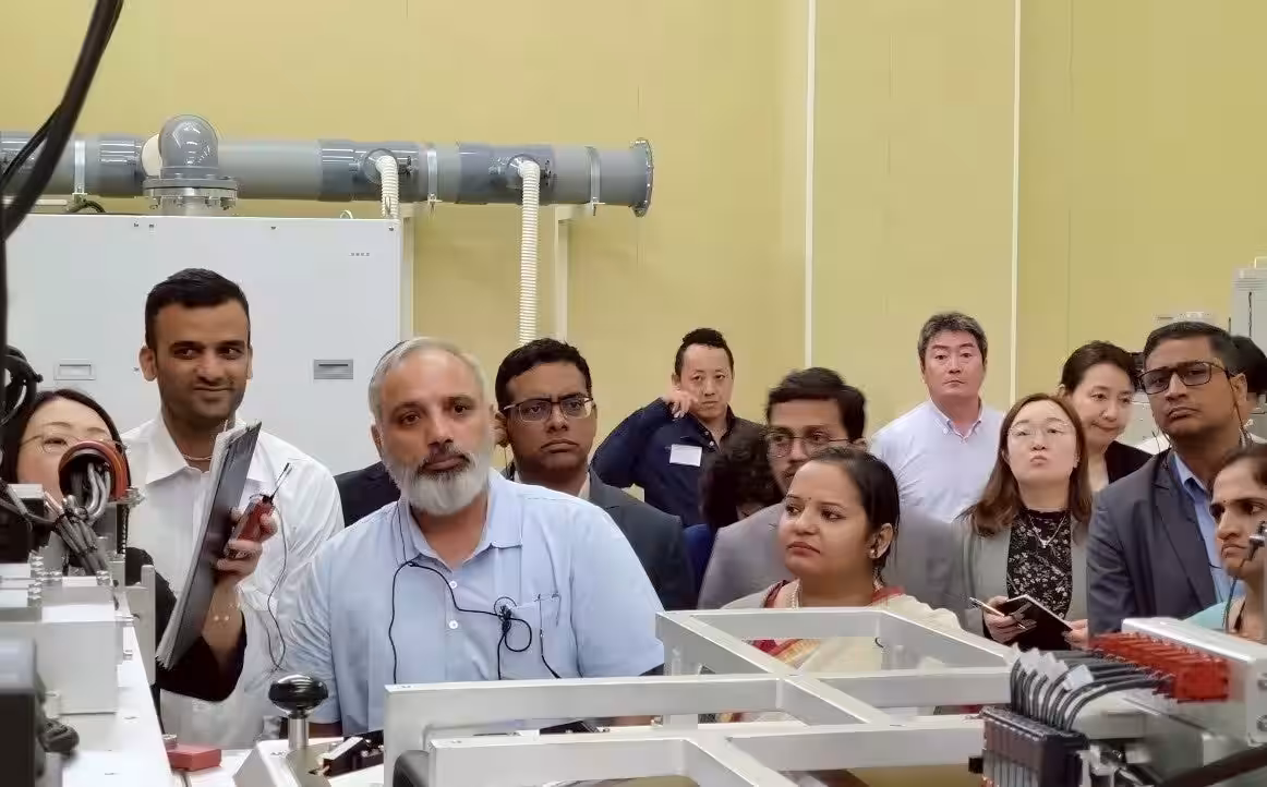
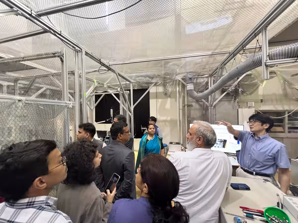
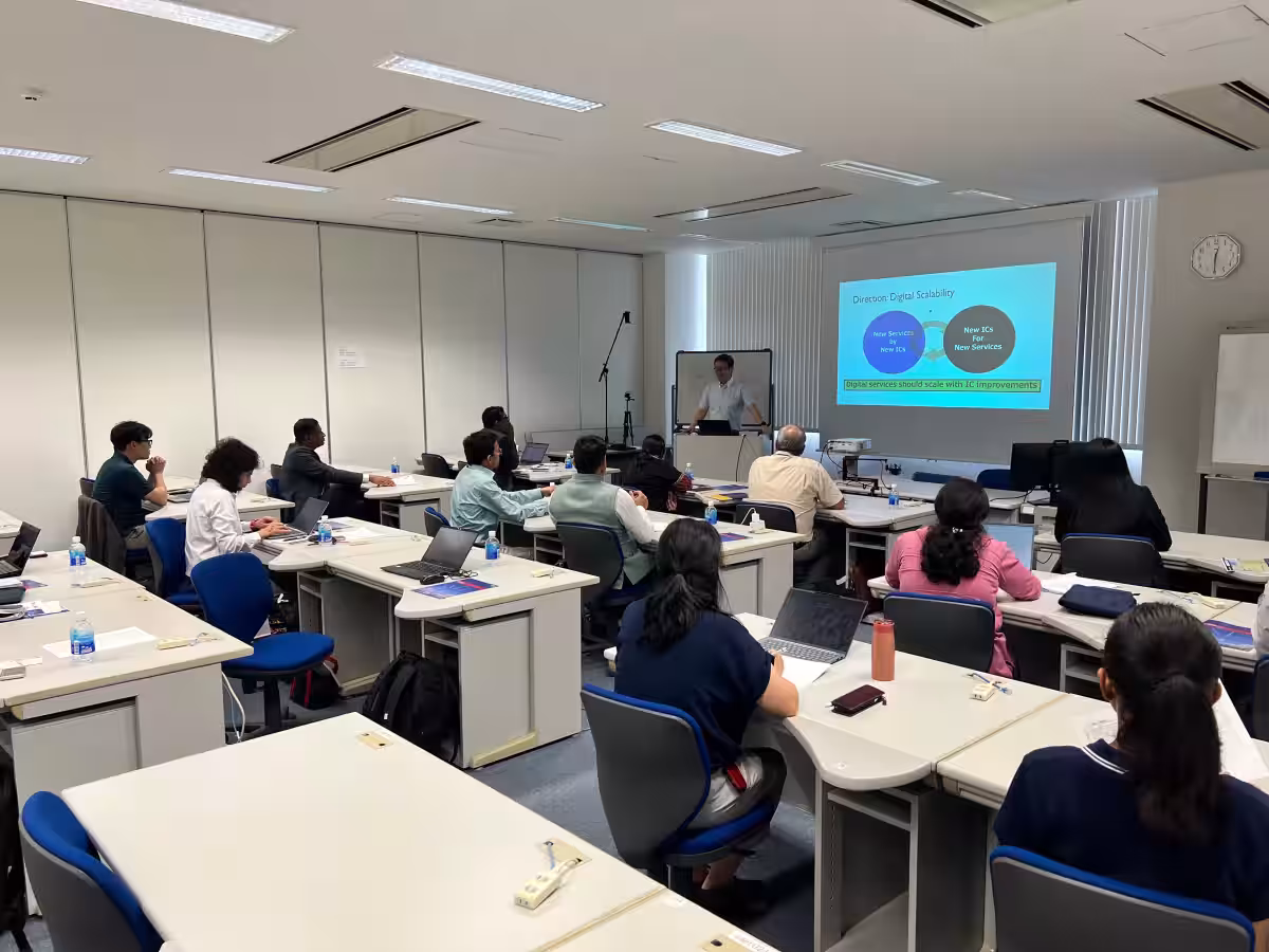
Fukuoka Semiconductor Reskilling Center - July 9
The reskilling center in Fukuoka presented a comprehensive array of semiconductor education tailored to meet industry needs. The Indian delegation showed great enthusiasm, engaging in a lively Q&A session that included over 20 questions. This active participation underscored a willingness to replicate similar educational models in India.
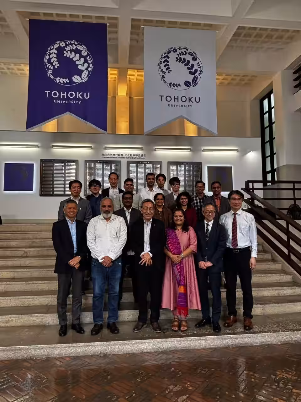
Tohoku University - July 10
The visit to Tohoku University included discussions regarding semiconductor policy in India and ongoing construction of domestic factories. The exchange of ideas led to discussions about fostering joint research and possible student exchanges between Tohoku University and Indian institutions.
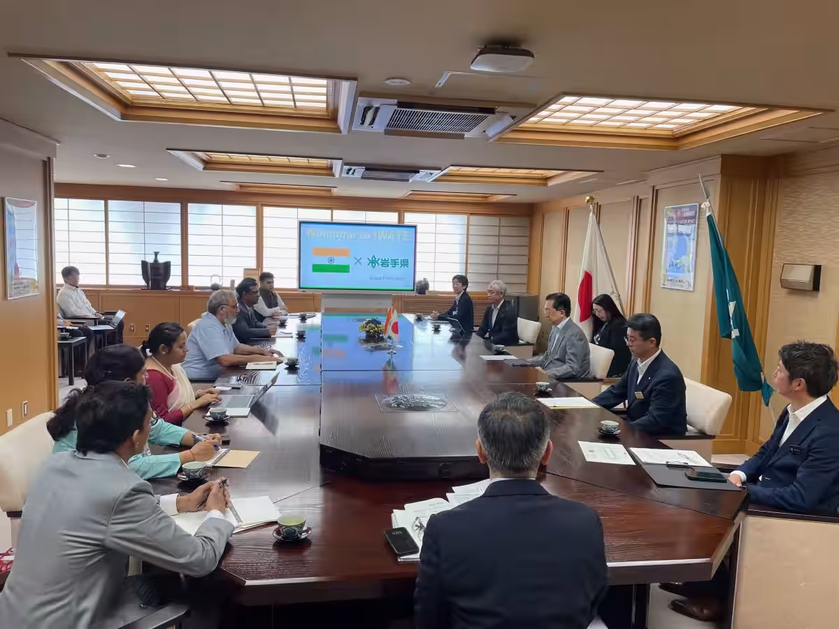
Iwate Prefectural Office - July 11
A courtesy meeting with Governor Takashi Tazawa at the Iwate Prefectural Office emphasized the importance of leveraging stable infrastructure and partnerships facilitated through the Iwate Semiconductor-Related Industrial Accumulation Promotion Council (I-SEP) for workforce development in India. This meeting reinforced the idea of mutual growth through collaboration.
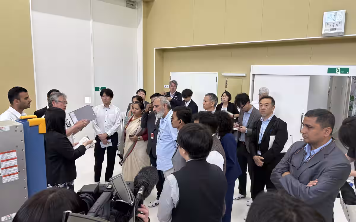
I-SPARK Semiconductor Workforce Development Facility - July 11
At I-SPARK, the delegation engaged with training sessions using semiconductor production equipment. They posed insightful inquiries about operational processes, showing commitment to utilizing this experience to enhance India's workforce development initiatives.
Kioxia Iwate Factory Visit
Finally, the visit wrapped up at the Kioxia facility, a leader in flash memory production, where discussions on the Japanese semiconductor industry's advancement took place. The exchange of insights contributed positively toward bilateral cooperation.
The Role of JICA
JICA plays a crucial role in implementing Japan's development assistance strategy globally, addressing challenges that many developing countries face. By promoting training and capacity-building initiatives, JICA further strengthens ties between Japan and India, aiming for enhanced global prosperity and mutual growth. For more details, visit JICA's official website.
Topics Consumer Technology)

【About Using Articles】
You can freely use the title and article content by linking to the page where the article is posted.
※ Images cannot be used.
【About Links】
Links are free to use.