


JASP Launches H&S HighTech Corp. Products in Japan: A New Era Begins
JASP Takes a Leap into the Japanese Market with H&S HighTech Corp.
Tokyo, Japan – JASP Corporation, based in Chiyoda, Tokyo, has officially commenced its full-scale sales and marketing operations for H&S HighTech Corp., a leading manufacturer of Anisotropic Conductive Film (ACF) from South Korea, in the Japanese market. This partnership marks a significant step towards enhancing the supply of advanced electronic materials in Japan.
H&S HighTech Corp.: A Global Player in Electronic Materials
H&S HighTech Corp. has been at the forefront of developing and manufacturing electronic materials for over 30 years, specializing in bonding materials for displays. The company has established itself as a top-three player in the global ACF market, supplying high-quality products to major display manufacturers and electronics firms worldwide.
In recent years, the demand for high-performance bonding materials has surged, owing to the expansion of sectors such as AI servers, high-performance semiconductors, data centers, and 5G communication devices. Recognizing this burgeoning market trend, H&S HighTech Corp. is accelerating its growth not only in the display materials sector but also in semiconductor packaging materials. They are actively developing innovative products like Build-up Film and the next-generation bonding material, Pattern Matching Film (PMF), to broaden their business horizons.
Understanding ACF and Its Importance
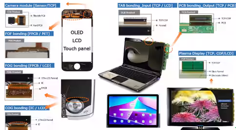
Anisotropic Conductive Film (ACF) plays a crucial role in connecting electronic components, semiconductor packages, flexible printed circuits, and display panels. It is widely used as a bonding material that simultaneously provides electrical connections and mechanical bonding.
ACF consists of a thermosetting resin film uniformly dispersed with conductive particles, achieving the following three essential functions:
1. Conductivity: Ensures electrical connectivity at the joint.
2. Insulation: Prevents short circuits between adjacent circuits.
3. Adhesion: Firmly secures components together.
Today, ACF is adopted extensively in various electronic devices, including LCDs, OLEDs, automotive displays, and camera modules.
Innovative Technology for Next-Gen Implementations
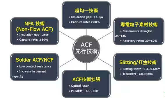
H&S HighTech Corp. is committed to advancing its unique ACF technologies tailored for next-generation electronic devices characterized by high-density assembly and Fine Pitch. Notable developments include:
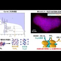
- - Hyper-even Distribution ACF: A technology that reduces resistance variation and short circuits by uniformly arranging conductive particles.
- - Non-flow ACF (NFA): A suitable solution for Fine Pitch assembly.
- - Solder ACF/NCF: Achieving low resistance and high current through metal bonding.
- - Direct Bonding Technology: Facilitating ultra-fine assembly for advanced applications.
These innovations ensure high-density assembly and reliable connectivity, essential for the evolving electronic landscape.
A Strategic Shift Towards Semiconductor Packaging Materials
Market research indicates that the semiconductor substrate materials market is projected to reach around 730 billion yen by 2031, driven by the growing demands of AI, data centers, and 5G infrastructure, with a compound annual growth rate of 19%. In response, H&S HighTech Corp. is investing actively in semiconductor packaging materials. They are progressing with the development of build-up films for semiconductor substrates and have introduced new technologies like PMF, focusing on enhancing innovations in semiconductor assembly.
Leveraging decades of expertise in display materials, H&S HighTech Corp. is steadily expanding its business to the semiconductor, AI, and data center-related sectors, carving out new growth avenues as an electronic materials manufacturer.
JASP's Role in the Japanese Market
JASP Corporation is responsible for the sales and technical support of H&S HighTech Corp.'s products in Japan. They aim to offer tailored ACF solutions based on specific applications and assembly requirements. JASP has established a comprehensive technical support system, providing assistance from prototype evaluation to mass production. This initiative will serve a wide array of sectors, including displays, electronic components, automotive devices, and semiconductor packaging, delivering high-quality bonding materials and technical expertise.
Moving forward, JASP is committed to introducing cutting-edge electronic materials and advanced technologies to the Japanese market, contributing to the innovation and competitive prowess of Japan’s manufacturing sector.
Topics Consumer Technology)


【About Using Articles】
You can freely use the title and article content by linking to the page where the article is posted.
※ Images cannot be used.
【About Links】
Links are free to use.