
Upcoming Seminar on Semiconductor Packaging Trends and Epoxy Materials Design and Evaluation


Upcoming Seminar on Semiconductor Packaging and Materials Design
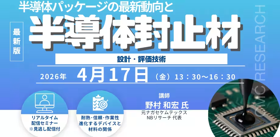
Join us on April 17, 2026, from 1:30 PM to 4:30 PM (JST) for a comprehensive seminar hosted by CMC Research, focusing on the latest developments in semiconductor packaging and the design and evaluation of sealing materials. This online event will be led by Kazuhiro Nomura, the representative of NB Research, ensuring an insightful experience for all participants.
Seminar Overview
The seminar aims to address the current trends in semiconductor packaging, particularly the increasing adoption of chiplet technology and 3D packaging. As these technologies advance, the demand for sophisticated sealing materials becomes apparent, necessitating advanced material design and evaluation techniques. Participants will gain practical knowledge in selecting raw materials, design methodologies, and techniques for reliability assessment, suitable for both new entrants and experienced professionals in the field.
What You Will Learn
- - The latest trends in semiconductor packaging.
- - Knowledge about raw materials used in sealing compounds.
- - Design techniques for sealing materials.
- - Evaluation methodologies for sealing materials.
The structured program will cover topics including various types of packaging, molding methods, the properties required for sealing materials, and evaluation tests that ensure quality and performance.
Target Audience
This seminar is designed for:
- - Engineers involved in the design of sealing compounds in semiconductors.
- - Technical professionals working with sealing materials.
- - Designers of epoxy resins and curing agents intended for use in semiconductor applications.
Registration and Fees
- - General Admission: 44,000 JPY (including tax)
- - Mailing List Members: 39,600 JPY (including tax)
- - Academic Rate: 26,400 JPY (including tax)
Participants are encouraged to register online through the CMC Research website. All registrants will receive a URL for streaming the seminar live via Zoom, along with access to an archival recording for a limited time.
Learn at Your Own Pace
If you are unable to attend live, don't worry! A recorded, on-demand version of the seminar will be provided. This allows you to revisit the content at your convenience, making it an excellent opportunity for comprehensive learning.
Seminar Agenda Highlights
The program will include:
1. Introduction to Semiconductor Packaging
- Types of packages: Wire Bond, Flip Chip, Wafer Level, and Advanced Packaging methods.
- Molding techniques: Transfer, Compression, and Dispensing Methods.
2. Design of Sealing Materials
- Raw materials: Epoxy resins, curing agents, and additives.
- Required properties for effective sealing materials.
3. Evaluation of Sealing Materials
- Individual evaluation tests and package-level assessments, including thermal-resistance and moisture-resistance tests.
4. Next-Generation Sealing Materials
- Trends in low dielectric and high thermal conductivity materials.
5. Q&A Session
- Engage directly with the speaker for a deeper understanding of the content discussed.
Why Attend?
Semiconductors play an essential role in various sectors, including automotive, medical, telecommunications, and AI. Given the increasing demand for miniaturization and high speeds in these areas, this seminar presents an invaluable opportunity to enhance your expertise in sealing materials, crucial for the next generation of semiconductor technologies.
Don’t miss out on this opportunity to expand your knowledge and connect with industry experts! For further details and to register, please visit CMC Research.
We look forward to welcoming you to this engaging seminar on the forefront of semiconductor technology advancements.
Topics Consumer Technology)
【About Using Articles】
You can freely use the title and article content by linking to the page where the article is posted.
※ Images cannot be used.
【About Links】
Links are free to use.