Unlocking the Future of Power Semiconductors in New Webinar by CMC Research


Upcoming Seminar on Power Semiconductor Evaluation Techniques
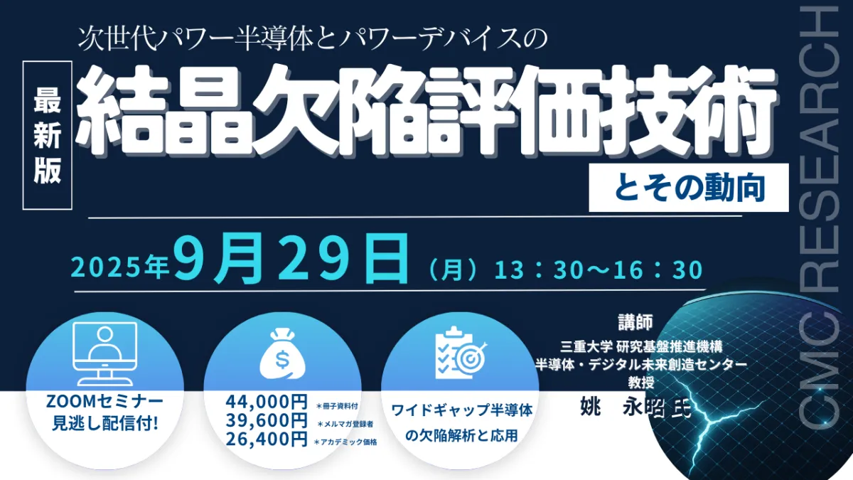
CMC Research is excited to announce a live webinar titled "Next-Generation Power Semiconductors and Power Devices Crystal Defect Evaluation Techniques and Trends," scheduled for September 29, 2025, from 1:30 PM to 4:30 PM (JST). This seminar will be hosted by Prof. Yao Yongzhao, a leading figure in semiconductor research from Mie University, focusing on the latest advancements in the evaluation of crystal defects in wide-bandgap semiconductors.
Why Attend?
This seminar is crucial for researchers and engineers involved in semiconductor crystal defect evaluation. It aims to provide participants with comprehensive knowledge regarding:
- - Crystal structures
- - Types of defects within crystals
- - Methods for evaluating these defects
- - The impact of defects on device performance
With the rapid developments in power devices using wide-bandgap semiconductors such as 4H-SiC, GaN, and β-Ga2O3, understanding defect analysis has become increasingly vital. These materials exhibit superior performance attributes, including high power density and stability at elevated temperatures. However, challenges arise due to the high density of lattice defects, which can significantly impair device reliability. By identifying killer defects through accurate defect distribution and type analysis, attendees will learn how to mitigate these issues, ensuring optimal device reliability and performance.
Seminar Agenda
The following topics will be covered during the webinar:
1. Introduction to Wide-Bandgap Semiconductors and Their Defects
- Understanding power device structures
- Significance of defect evaluation methods
2. Exploration of Defect Evaluation Techniques
- Selective chemical etching (etch pit method)
- Transmission Electron Microscopy (TEM)
- Multi-photon excitation microscopy
- X-ray diffraction and topography
3. Assessment of Devices and Their Defects
- Types of defects in devices
- Methods for evaluating defects in devices
- Adverse effects of defects on device performance
4. Summary of Key Learnings
Interactive Session
An interactive Q&A session will follow the presentations, allowing participants to engage directly with Prof. Yao and gain insights into the complexities of semiconductor technology.
Participation Fees
- - General Participants: ¥44,000 (tax included)
- - Newsletter Subscribers: ¥39,600 (tax included)
- - Academic Participants: ¥26,400 (tax included)
Additional Features
For those unable to attend the live session, we will provide an archivable playback option, allowing access to recorded sessions for a limited time. This ensures that all interested parties have the opportunity to learn at their convenience.
Enrollment
To register for the webinar, please visit the CMC Research seminar page. After registration, participants will receive a separate email with a viewing URL.
This seminar serves as an opportunity to connect theoretical research with practical applications, enhancing the knowledge required for cutting-edge semiconductor technology. Join us in exploring the avenues toward the next wave of innovations in the semiconductor industry!
For more details and registration, click here.
Topics Consumer Technology)
【About Using Articles】
You can freely use the title and article content by linking to the page where the article is posted.
※ Images cannot be used.
【About Links】
Links are free to use.