


Toray Research Center Launches Innovative Analysis Service to Visualize Current Pathways in Layered Devices
Introduction
Recently, the Toray Research Center (TRC), based in Chuo, Tokyo, has taken a pioneering step in the field of semiconductor and organic devices by launching an innovative service that visualizes how current flows within layered devices. This groundbreaking analysis service integrates various surface analysis techniques to evaluate the composition and chemical states of materials, as well as the energy states relevant to charge transport throughout the device's structure.
The Importance of Current Pathways
The development of layered devices, which are widely used in semiconductors, organic EL displays, and solar cells, is crucial for advancing technologies in AI, mobility, and telecommunications. These devices operate by enabling the movement of charges, such as electrons and holes, across multiple functional layers. The ease with which these charges can migrate directly affects overall device performance. Therefore, understanding the electronic properties that govern the 'pathways' of current flow is vital for optimizing device efficiency.
Traditionally, while elemental composition and chemical states could be assessed, it remained challenging to analyze the electronic states controlling charge transport across differing layers and interfaces. This limitation hindered accurate diagnosis of performance variances and identifying causes of degradation.
Overview of the New Service
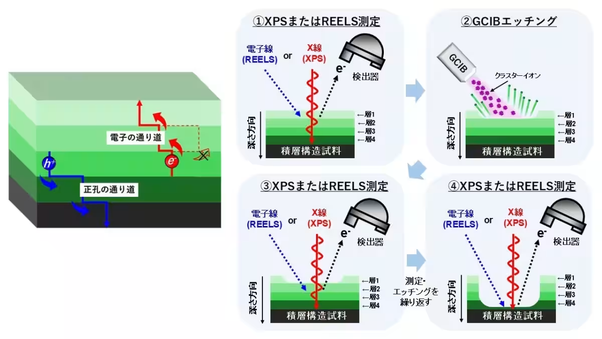
To tackle these challenges, TRC has developed an advanced surface analysis service that uses a gas cluster ion beam (GCIB) to mill sample surfaces at the nanometer scale while simultaneously conducting measurements such as X-ray photoelectron spectroscopy (XPS) and reflection electron energy loss spectroscopy (REELS). This allows for comprehensive analysis of electronic states in each layer and at the interfaces of layered devices.
Key Features of the Service
- - Quantitative Visualization: Ability to visualize the electronic energy states quantitatively for each layer and interface.
- - Micro-region Analysis: Capable of analysis within small areas applicable to real devices.
- - Minimal Damage: By minimizing damage during measurement, the service can be applied even to structures involving organic materials.
- - Correlation Analysis: Allows correlation of electronic states with composition and chemical states through analysis in the same region.
Illustration showing the layered structure of a device and the pathways for electron and hole movement (left) and a simplified diagram of the analysis procedure combining GCIB-XPS and GCIB-REELS measurements (right).
Future Developments
The recent service introduction aims to enhance the understanding of performance variations and defects in semiconductor devices and to clarify the mechanisms behind the degradation and performance enhancement of organic EL displays and solar cells. This will facilitate the acquisition of design guidelines for developing new materials and structures, ultimately contributing to improved development efficiency and enhanced device performance.
As the demand for high performance and low power consumption rises in advanced device sectors, evaluating electronic states becomes crucial for addressing these challenges effectively. TRC remains committed to providing analytical services that tackle issues in semiconductors, displays, and energy devices.
Terminology Explained
- - Electronic States: Refers to the energy distribution and levels of electrons, crucial factors determining the migration ease of charges (electrons and holes).
- - GCIB: A technology that involves ionizing clusters of numerous atoms to mill the surface at the nanometer scale, causing less damage than single-atom ions, preserving interface structures even in organic materials.
- - XPS: A method that irradiates surfaces with X-rays and measures the energy of emitted photoelectrons to assess elemental composition, chemical states, and electronic states.
- - REELS: An analytical technique that uses electron beams to illuminate a sample surface and measure the energy of emitted electrons to derive insights about its electronic structure, such as band gaps.
Topics Consumer Technology)


【About Using Articles】
You can freely use the title and article content by linking to the page where the article is posted.
※ Images cannot be used.
【About Links】
Links are free to use.