
Successful Fabrication of High-Quality ScAlN Films Using Sputtering Method Revealed Impact of Growth Temperature


Introduction
The research team led by Associate Professor Atsushi Kobayashi from the Tokyo University of Science has achieved significant advancements in the fabrication of high-quality ScAlN (Scandium Aluminum Nitride) films using a widely applicable sputtering method. This marks a pivotal moment in materials science and semiconductor technology as it opens new avenues for the development of next-generation electronic devices.
Overview of the Research
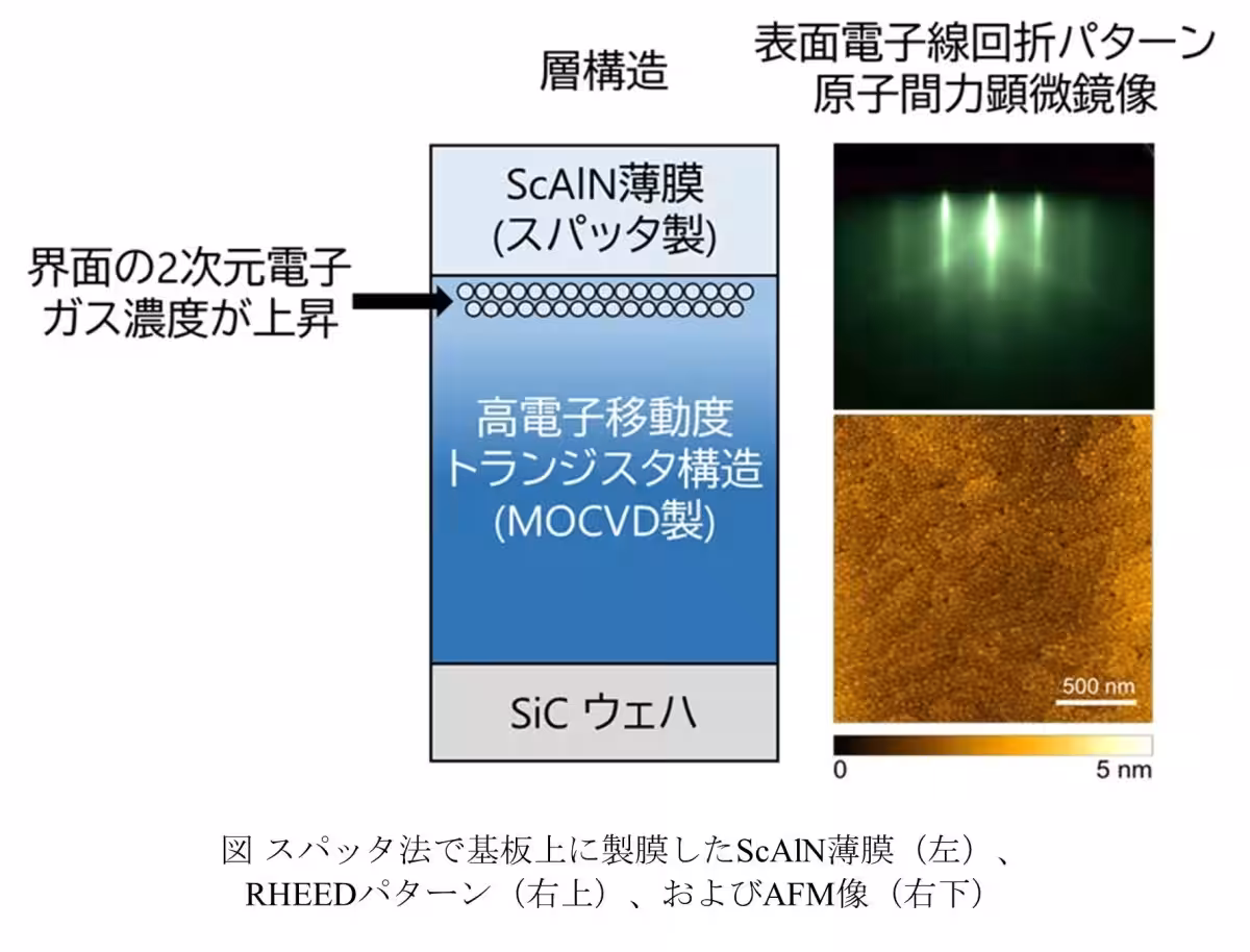
High-quality ScAlN films have long been considered challenging to create due to the complex crystal growth required. The team's findings demonstrated that increasing the growth temperature resulted in improved surface flatness, with films grown at 750°C exhibiting the best characteristics. Notably, these films achieved an impressive two-dimensional electron gas (2DEG) density of approximately three times (1.1 × 10¹³ cm⁻²), indicating a promising application in high-performance electronic devices.
This innovative sputtering technique not only simplifies the fabrication process but also holds the potential to be applied to various nitride semiconductor materials, thereby making a significant impact across the entire electronics field. The collaborative efforts with The University of Tokyo (conducting electrical property measurements) and Sumitomo Electric Industries (producing HEMT wafers) emphasize the research's industrial relevance.
Importance of ScAlN
ScAlN is notable for its high piezoelectric coefficients and spontaneous polarization, making it an excellent candidate as a barrier material for GaN-based high electron mobility transistors (HEMTs). Additionally, its ferroelectric properties offer promising opportunities for applications in non-volatile memory and multifunction devices. However, challenges such as crystal structure disorder and degraded interface quality due to Sc addition have historically hampered electron mobility.
The Sputtering Method
The team focused on utilizing the sputtering method, which tends to be simpler and more cost-effective than traditional techniques like molecular beam epitaxy (MBE) and metal-organic chemical vapor deposition (MOCVD). They conducted a systematic investigation of how varying growth temperatures (250–750°C) affected the film quality and electrical properties of the ScAlN films grown on AlGaN/AlN/GaN/SiC substrates.
Structural Analysis
The team's experimental results revealed that as the growth temperature increased, the surface of the ScAlN films became smoother, with the highest quality achieved at 750°C. Using reflection high-energy electron diffraction (RHEED), they confirmed that epitaxial growth was feasible even at low temperatures (250°C), while higher temperatures showcased improved atomic arrangement. Atomic force microscopy (AFM) analysis indicated that the films underwent step-flow growth, displaying distinct steps and terraces at elevated temperatures.
Notably, X-ray diffraction (XRD) data illustrated that the ScAlN films maintained lattice matching with the substrates across the entire temperature range, reducing the c-axis lattice constant as growth temperatures increased. This suggests that thermal activation at high temperatures facilitated better atomic rearrangement, leading to less lattice strain in the c-axis direction.
Electrical Evaluation
Analyzing the electrical properties via Hall effect measurements, the researchers found that the sheet carrier density in the structure significantly depended on the growth temperature. The film produced at 750°C displayed a carrier density of 1.1 × 10¹³ cm⁻², approximately three times that of the pre-deposited density. However, while the carrier density improved, the electron mobility decreased due to roughness at the interfaces and structural imperfections. This highlights the delicate balance between achieving high carrier density and maintaining optimal electron mobility.
Professor Kobayashi commented on the significance of their findings, emphasizing that the successful fabrication of high-quality ScAlN films using the sputtering method could accelerate the development of high-performance and environmentally resilient electronic devices.
Conclusion
The research not only succeeds in confirming that growth temperature is a crucial parameter impacting both the quality of ScAlN films and their 2DEG characteristics, but also underscores the feasibility of utilizing sputtering techniques in the field of high-quality semiconductor development. The established framework can potentially lead to the realization of next-generation electronic devices, enhancing efficiency and performance in various applications. The research has been recognized as an 'Editor’s Pick' in the international journal APL Materials, underscoring its importance and impact.
Acknowledgements
This research was conducted with support from the Japan Society for the Promotion of Science (JSPS) and various foundations focused on scientific advancement.
Future Directions
Moving forward, the insights gained from this research are anticipated to fuel ongoing investigations into the potential applications of ScAlN in diverse electronic devices, further bridging the gap between advanced materials science and practical technology.
Topics Consumer Technology)
【About Using Articles】
You can freely use the title and article content by linking to the page where the article is posted.
※ Images cannot be used.
【About Links】
Links are free to use.